

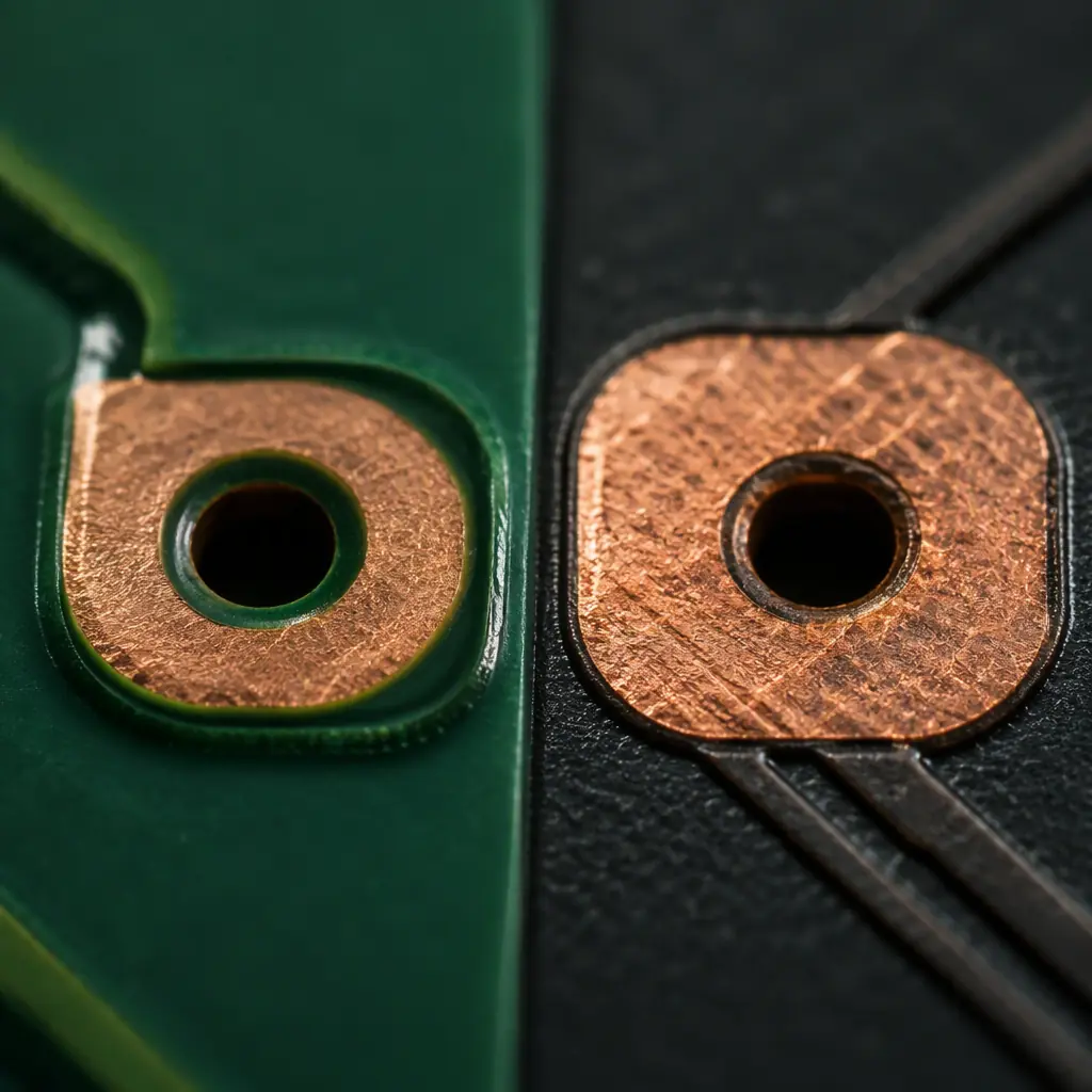
Every pad on a PCB sits inside a solder mask opening. The question is how the opening relates to the copper pad underneath. If the copper pad is larger than the mask opening, the mask overlaps onto the copper and the exposed metal, the area the solder can actually wet, is the part inside the opening. That is a non-solder-mask-defined (NSMD) pad. If the mask opening is smaller than the copper pad, so the mask lands inside the pad and leaves a rim of copper “shoulder” under the mask, that is a solder-mask-defined (SMD) pad. It is a small geometry difference with a large effect on reliability, fine-pitch work and manufacturability. At Huaxing PCBA we run 3/3 mil trace and space, 0.15 mm minimum hole and 0.5–6 oz copper on 32-layer boards, so we set pad geometry on a daily basis.
What Actually Defines SMD vs NSMD
The distinction comes down to one relationship: the size of the copper pad versus the size of the solder mask opening. It is usually expressed as the mask opening and the copper pad in the design.
| Pad type | Copper vs mask opening | Exposed solderable area |
|---|---|---|
| NSMD | Copper > opening | Full copper pad, mask overlaps the edge |
| SMD | Opening < copper | Opening area only, copper shoulder under mask |
NSMD is the default for most designs because the whole copper pad is exposed, giving the largest solderable area. SMD is a deliberate choice for specific footprints where you want the copper shoulder to do mechanical or electrical work. The names are easy to confuse, “solder-mask-defined” means the mask defines (limits) the solderable area.
NSMD: Bigger Wetting, Better for Fine Pitch
An NSMD pad exposes the full copper pad, so you get the maximum surface for the solder to wet and the most consistent joint. As pitch tightens toward 0.3 mm BGAs and 0201 passives, NSMD is almost always the right answer.
Largest solderable area
Because nothing covers the pad, the full copper area is available to the solder, which maximizes wetting and reduces the chance of an open or a weak joint on fine-pitch terminals.
Lower crack risk at the pad
The solder joint neck is wider, and there is no copper shoulder to act as a stress-riser on the pad edge. Under thermal cycling the crack path is less likely to concentrate at the pad boundary. See our thermal cycling and signal integrity guides for the downstream effects.
Preferred for tight pitch
Fine-pitch BGAs and QFNs are specified as NSMD because the mask registration cannot be controlled tightly enough at 0.3 mm pitch to reliably define the pad. The copper registration is better than mask registration, so NSMD is the safe choice.
SMD: The Copper Shoulder and Where It Wins
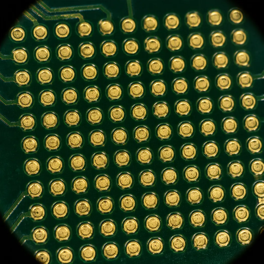
An SMD pad leaves a ring of copper under the mask around the exposed opening. That shoulder adds two things: a mechanical anchor and a wider thermal path. It is why SMD is still used for certain pads even though NSMD is the default.
Better pull-off / shear strength
The mask-anchored copper shoulder resists a pad being lifted off the board, which helps with small pads and with anything that suffers mechanical stress. This can matter for small passives in a vibration-prone application.
Helps with mask registration tolerance
Because the opening can be made slightly smaller than the pad, an SMD pad gives a little more tolerance to mask mis-registration, which historically made it a common choice for through-hole footprints and older processes. It is less relevant at modern fine pitch.
The thermal / current trade-off
An SMD pad exposes less copper, so it has a smaller effective thermal and current area under the mask. That is fine if the joint is not the main thermal path, but wrong if you are counting on the pad to spread heat. See our trace current capacity and copper weight selection guides.
Where it can hurt
On a fine-pitch pad an SMD opening can create a solder mask defined joint that is narrower than the pad, which raises the crack risk and can starve the wetting. That is the classic reason not to use SMD on very fine-pitch QFN or BGA terminals.
Where Each Pad Type Belongs
The rule of thumb is simple: the tighter the pitch and the more the joint depends on wetting, the more you want NSMD; the more you need mechanical strength or are not thermal-limited, the more SMD can help.
| Component / scenario | Best pad type | Reason |
|---|---|---|
| Fine-pitch BGA / QFN (≤0.4mm) | NSMD | Copper registration beats mask registration |
| 0201 / 0402 passives | NSMD | Biggest wetting, smallest part |
| Large power pad / thermal pad | NSMD or SMD | NSMD for max thermal, SMD if pull-off strength dominates |
| Small pads in a vibration-prone product | SMD | Copper shoulder resists lift-off |
| Through-hole / pad for hand solder | SMD | Registration tolerance historically |
Reliability: The Crack Path and Thermal Cycling
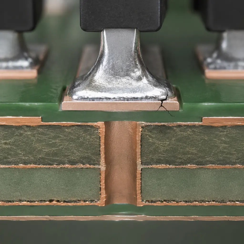
Where the two pad types really diverge is in the crack path under thermal cycling and mechanical stress. With SMD, the interface sits at the mask edge, and a smaller exposed area means a smaller, weaker solder neck, the crack tends to start at the pad edge under the mask. With NSMD, the joint is fuller and the crack is less likely to initiate at the pad boundary, so the life is generally longer for the same solder volume. For a board that has to survive hundreds or thousands of thermal cycles, that difference is often the deciding factor.
The practical implication is that NSMD is the safer default for anything that cycles, and SMD should be reserved for the cases where the mechanical strength of the copper shoulder genuinely buys you something. See our thermal management and warpage guides for how the two interact in high-stress designs.
Manufacturability and What to Ask For
Pad type is set in the CAD file, but it shows up in the fab and the assembly. Ask your supplier to confirm the pad geometry they are building to and that the mask opening matches the design intent.
Mask registration
NSMD relies on the copper pad being fully exposed, so the mask opening has to clear the pad edge. If the mask is registered badly, it can intrude onto the pad and reduce the solderable area. Confirm the mask registration spec and the opening-to-pad clearance.
Photo-defined vs window mask
SMD pads need the mask to land precisely on the copper, which puts more demand on the mask process. Your supplier should be able to hold the mask registration that 3/3 mil line and space demands.
Design-for-manufacturability check
Run a DFM pass on the footprint before you commit. The difference between NSMD and SMD is a few tens of microns, and a DFM review catches a choice that is inconsistent with the rest of the board. See our DFM rules and tolerances guides.
Procurement Tip: If your board has a leadless power package, a fine-pitch BGA or a mix of both, ask the supplier which pad type they assume, and to flag it in the DFM review. A design drawn as NSMD that is built as SMD, or the reverse, changes the joint and the reliability of the board.
The Right Choice Is Usually NSMD
Modern practice points to NSMD as the default for dense, fine-pitch, high-reliability boards, with SMD reserved for the specific mechanical-strength or registration cases above. The decision is not cosmetic; it changes the solder joint, the thermal path and the service life. When in doubt, and especially when a single board mixes 0201 passives, a 0.3 mm BGA and a power pad, run the footprint through a DFM review and let the supplier confirm the pad type against their process.
At Huaxing PCBA we build 2–32 layer boards with 3/3 mil line and space, 0.15 mm minimum holes and 0.5–6 oz copper, and we run a free DFM review on every order with your 0201 and 0.3 mm pitch placement across 8 SMT lines and 8M placements/day in a 15,000 m² facility. We are ISO 9001, IATF 16949 and UL (E354321) certified with 99.2% on-time delivery. Upload your design or ask our engineering team about your pad and footprint choices. For related reading, see our stackup design and signal integrity guides.
