
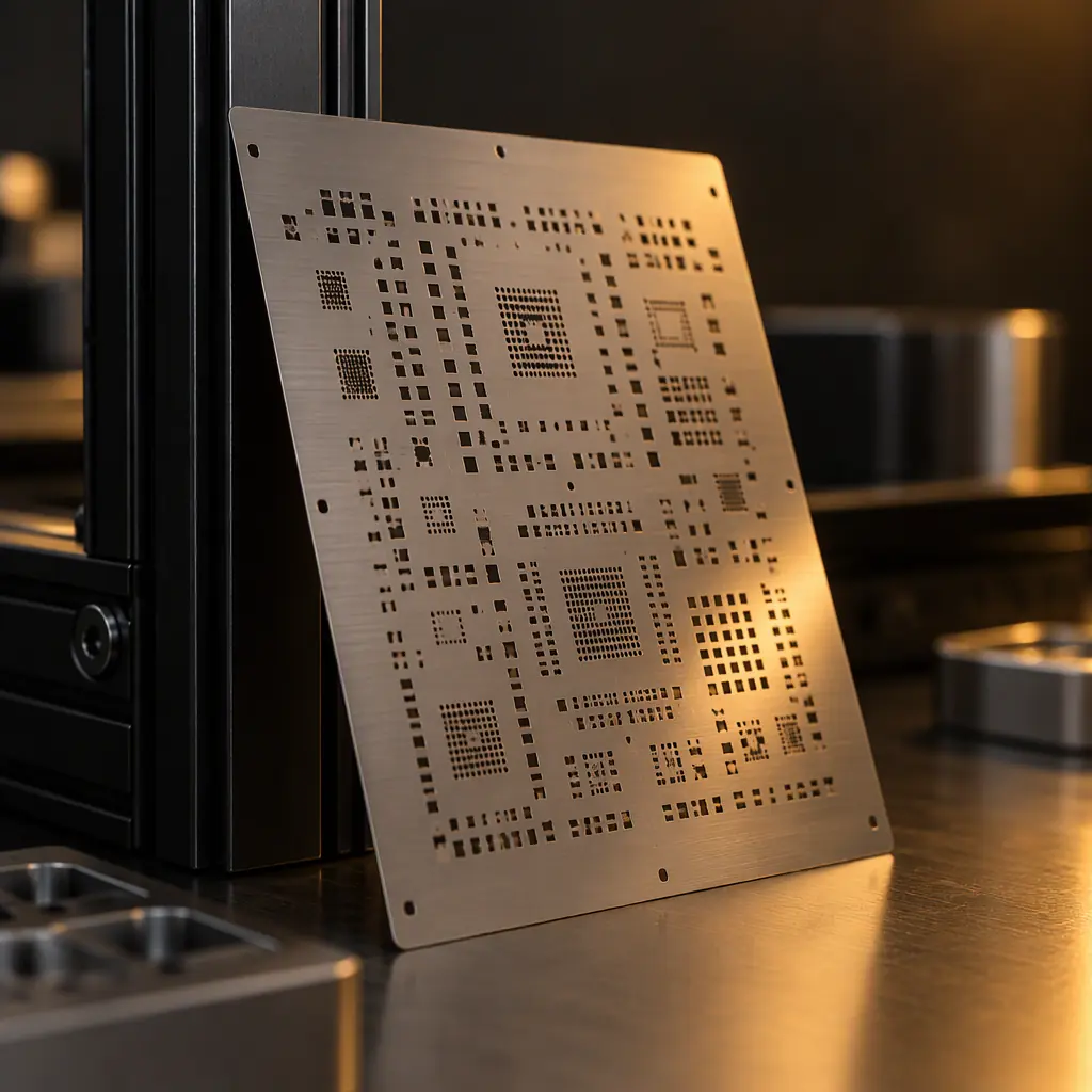
The stencil is the only volume-dispensing device on a solder paste printing line. Every other input that printers argue about, squeegee pressure, print speed, separation speed and cleaning frequency, only decides how faithfully the apertures in that thin metal sheet get filled and emptied. Thickness decides how much paste is available to be printed at all. Where the sheet is too thin for the pad and the part, no amount of pressure tuning will fix the joint; the printer is being asked to place 60 percent of the paste the joint needs.
Most buyers and many process engineers specify thickness by habit: 120 micron for fine pitch, 150 micron for general work, 180 or 200 micron for power boards. That habit is not wrong, but it is not derived. It breaks exactly when the board mixes fine pitch with heavy thermal pads, which is most modern mixed-technology assemblies. This page covers the derivation, the arithmetic, and the inspection records that show whether the number in the purchase order was actually used.
Our stencil aperture design and paste release guide covers the area ratio rule and how aperture geometry interacts with the foil; this page is the volume side of the same physics. If you are still deciding whether a stencil is the right tool at all, the jetting versus stencil cost comparison covers the break-even.
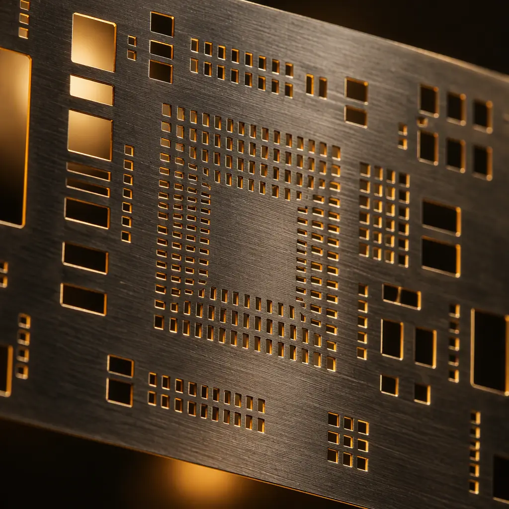
Foil thickness is the one print variable fixed before the line starts. Everything the printer adjusts is downstream of it.
What Foil Thickness Actually Determines
Foil thickness multiplied by aperture area gives the nominal paste volume deposited per pad. That single multiplication is why thickness selection is a design decision and not a machine setting. A 0.50 mm by 0.50 mm aperture in 100 micron foil holds 0.025 cubic millimetres of paste. The same aperture in 150 micron foil holds 0.0375 cubic millimetres, a 50 percent increase. No squeegee adjustment can add that difference back if the foil is too thin.
The joint needs a specific volume. A joint that receives too little paste reflows into a fillet that is concave, thin and prone to cracking under thermal cycling. A joint that receives too much paste does not simply look fat; it lifts the component, forms beads beside the pad, and in fine pitch it bridges. Thickness, therefore, has both a floor and a ceiling at the same time, and the usable band for a mixed-technology board is often narrower than a single gauge can satisfy.
Thickness also constrains what the surface can release. Paste is a non-Newtonian suspension; it needs enough aperture wall area for adhesion to keep it in place, and enough depth for the release force to act on. A thick foil in a small aperture releases better than a thin foil in the same aperture, because the area ratio is the ratio of aperture pad-area to aperture wall-area, and wall area is thickness times aperture perimeter. Increasing thickness improves area ratio while reducing print resolution on fine pitch, which sets up the trade-off every process engineer works through.
| Foil thickness | Typical use | Practical minimum aperture (0.66 area ratio) | Paste volume per 0.4 x 0.4 mm pad | Constraint it introduces |
|---|---|---|---|---|
| 80 micron | 0.4 mm pitch and finer, 01005 and 0201 | 0.155 mm | 0.0128 mm3 | Very low hydrostatic pressure; paste sticks; needs nano-coating |
| 100 micron | 0.4 mm pitch fine pitch, 0.35 mm CSP | 0.195 mm | 0.0160 mm3 | Thin paste columns; bridges form from post-release slump |
| 120 micron | 0.5 mm pitch QFN and general fine pitch | 0.235 mm | 0.0192 mm3 | Common default; often marginal on 0.4 mm pitch thermals |
| 130 micron | Mixed pitch 0.4 to 0.8 mm | 0.254 mm | 0.0208 mm3 | Compromise gauge; verify on both extremes |
| 150 micron | 0.65 mm pitch and above, general SMT | 0.294 mm | 0.0240 mm3 | Too much paste on 0402 pads; beading risk |
| 180 micron | Power devices, 1206 and larger pads | 0.353 mm | 0.0288 mm3 | Cannot print fine pitch at all; step needed |
| 200 micron | Through-hole pin-in-paste, large thermal tabs | 0.392 mm | 0.0320 mm3 | Severe slumping on any small pad under 0.5 mm |
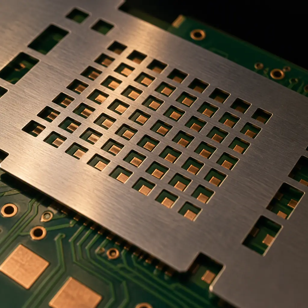
The finest aperture on the board, not the average, decides the thickness ceiling.
Deriving the Number From Joint Volume
The correct starting point is not thickness; it is the volume the joint needs. That volume comes from three inputs: the pad area on the board, the standoff height the component will sit at, and the amount of paste that collapses into the barrel of any plated through hole in a pin-in-paste design.
For a surface mount pad, the required paste volume is the cuboid above the pad: pad area multiplied by the paste height, where paste height after reflow is set by the component termination and the solder fillet requirement. In practice, reputable calculators use 50 to 60 percent of the foil thickness as the effective release volume for a normal aperture. The rest of the paste is retained on the aperture wall or left behind as a thin film on the board surface around the deposit.
Worked example, an 0805 chip resistor. The pad is 1.40 mm by 1.15 mm. At 150 micron foil, nominal volume is 1.40 x 1.15 x 0.150 = 0.2415 mm3 per pad, and at a 55 percent release that is roughly 0.133 mm3 of actual paste per pad. The joint for an 0805 termination typically wants 0.050 to 0.090 mm3 of solder. At 150 microns the pad is supplied with more paste than the joint can absorb, and the surplus becomes the solder bead beside the part. This is the mechanism behind a defect class that usually gets blamed on paste rheology.
The same calculation at 120 micron gives 0.1932 mm3 nominal and about 0.106 mm3 released, still on the generous side. At 100 micron it gives 0.161 mm3 nominal and 0.089 mm3 released, which sits at the top of the band. For an 0805 the comfortable thickness is 100 to 120 micron, and the same board with a 0.5 mm pitch QFN on it will want 120 to 130. That convergence is why 120 micron became the default: it is the gauge that is defensible for both.
The through-hole correction
Pin-in-paste changes the arithmetic completely. Paste must fill the barrel of the through hole and form a fillet on both sides. A 1.0 mm finished hole in 1.6 mm board takes 1.26 mm3 just to fill the barrel. Aperture area on a 2.0 by 2.5 mm annular pad is 5.0 mm2, so at 55 percent release the foil must be at least 1.26 / (5.0 x 0.55) = 0.46 mm thick to deliver barrel fill from the print alone, which no printable foil reaches. This is why pin-in-paste requires either extra aperture area beyond the pad (paste over the hole, with a relief pocket in the stencil), a thick step, or acceptance that the joint is filled from a wave or selective solder pass.
The one-line rule we use at recipe review
Thickness is set by the smallest aperture and the largest hole on the same board. If those two requirements differ by more than one gauge, the board needs a stepped stencil, not a compromise gauge. A compromise gauge always fails on the narrow side, because the fine pitch defect is silent until electrical test.
Area Ratio and Aspect Ratio Limits by Thickness
Area ratio is aperture opening area divided by aperture wall area. For a rectangular aperture of width W and length L in foil of thickness T, it is (W x L) / (2 x T x (W + L)). Aspect ratio is the simpler W / T. Industry practice treats 0.66 as the practical minimum for consistent release and 0.60 as the point where the process depends on coating, paste type and operator attention. These two ratios move in opposite directions with thickness, which is the whole reason thickness cannot be optimised globally.
| Aperture width (square) | Area ratio at 100 µm | at 120 µm | at 150 µm | at 180 µm | Verdict |
|---|---|---|---|---|---|
| 0.40 mm | 1.00 | 0.83 | 0.67 | 0.56 | Prints at 150 with attention; step down for margin |
| 0.30 mm | 0.75 | 0.63 | 0.50 | 0.42 | Needs 120 or thinner; 150 is marginal |
| 0.25 mm | 0.63 | 0.52 | 0.42 | 0.35 | 100 max |
| 0.20 mm | 0.50 | 0.42 | 0.33 | 0.28 | 80 µm foil plus nano-coating only |
| 0.15 mm | 0.38 | 0.31 | 0.25 | 0.21 | Below practical limit in stainless; electroform or jetting |
| 1.00 mm | 2.50 | 2.08 | 1.67 | 1.39 | All gauges release; volume becomes the constraint |
Read the table from left to right and it becomes a selection chart. A board whose finest aperture is 0.30 mm square cannot use 150 micron foil at 0.66 area ratio; it lands at 0.50. A board whose finest is 0.40 mm is exactly at the line with 150 micron. Most datasheets quote area ratio against a nominal thickness, and the number quietly changes when the thickness changes.
Length matters too, and it is easy to forget. A 0.30 mm by 1.50 mm rectangular aperture has an area ratio of 0.75 at 150 micron, worse than a 0.30 mm square, because the wall area grows with the long side. Long thin apertures, common on QFN thermal pad segmentation and on connector pin rows, are the apertures that fail first on a step stencil.
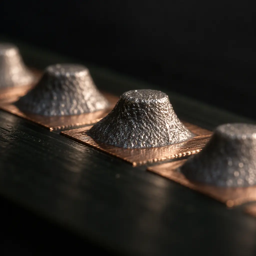
Wall retention is visible in deposit shape: a paste column with sloped sides indicates that part of the volume stayed on the aperture wall.
Transfer Efficiency by Aperture Size and Thickness
Nominal volume is a calculation; actual volume is a measurement. Transfer efficiency is actual divided by nominal, and it falls as apertures shrink. At large apertures and any practical gauge, efficiency sits between 90 and 100 percent. It crosses 80 percent around 0.4 mm apertures in 120 micron foil, 65 to 75 percent around 0.30 mm, and 50 to 60 percent at 0.20 mm. Those losses must be planned for, not discovered.
Two effects cause the loss. First, adhesion between paste and aperture wall retains material, and the retained fraction grows as wall area grows relative to opening area, which is exactly the area ratio. Second, the release event itself, foil peeling away from the board at the separation speed, creates a local vacuum in the aperture that pulls paste from the deposit. Apertures with a high area ratio release cleanly and leave a flat-topped deposit. Apertures at the limit leave a deposit with a concave top and paste smeared on the wall.
| Aperture (square) | Nominal volume, 120 µm foil | Expected transfer efficiency | Actual volume | Deposit appearance |
|---|---|---|---|---|
| 0.60 mm | 0.0432 mm3 | 92 to 98 percent | 0.0401 mm3 | Flat top, sharp edges |
| 0.40 mm | 0.0192 mm3 | 80 to 90 percent | 0.0163 mm3 | Flat top, slight wall film |
| 0.30 mm | 0.0108 mm3 | 65 to 75 percent | 0.0076 mm3 | Slightly concave top |
| 0.25 mm | 0.0075 mm3 | 55 to 68 percent | 0.0046 mm3 | Concave, visible smear |
| 0.20 mm | 0.0048 mm3 | 45 to 60 percent | 0.0026 mm3 | Inconsistent height, torn deposits |
This is where a volume calculation done on nominal foil thickness goes wrong. A design that assumes 100 percent transfer at 0.25 mm aperture will under-supply every joint by close to 40 percent and the failure will appear not at print but at final test, as intermittent opens on a component that looked fine at AOI, because the AOI was set using the same optimistic nominal.
Stepped Stencils: Where They Are Required
A stepped stencil changes thickness locally, either by laser welding a foil patch or by electroforming a single piece with regions of different thickness. It exists precisely because one gauge cannot serve a mixed-technology board. The cost is real and the lead time is longer, so the decision to use one should be made on evidence.
Mixed pitch below and above the 0.66 line
If the board carries a 0.4 mm pitch QFN with 0.25 mm apertures alongside an 0.8 mm pitch connector needing 150 micron in a 0.6 mm aperture, the two requirements do not overlap. A step from 100 to 150 micron satisfies both. A single 120 gauge satisfies neither well.
Pin-in-paste alongside fine pitch
Through-hole connectors that need 200 micron paste volume on 2.0 mm pads, next to fine pitch SMT that cannot tolerate more than 120 micron, is the classic step case. Without the step, the fine pitch beads and the through hole starves.
Thermal pads that need more paste than a fine pitch gauge allows
A QFN thermal pad is a large aperture with a low area ratio problem in reverse: it releases easily but needs volume. Segmentation and a step in the thermal region solve both the paste volume and the voiding that comes from a single large deposit.
Small boards with a few large pads on a panel
Panel-level stepping is possible but must be designed at panelisation. A step that crosses panel rails causes squeegee drag and should be planned around the array, not retrofitted.
A step has two practical costs that do not appear on the quote. First, the squeegee must climb or descend a foil edge; a badly placed step catches paste and creates a smear trail across several apertures. Steps must be placed in an area with no apertures for at least 2 mm on each side. Second, the step face wears. Foil with a step is retired earlier than flat foil, so the lifecycle counter must account for it, which is why the stencil lifecycle and retirement criteria are more important on stepped tools than on flat ones.
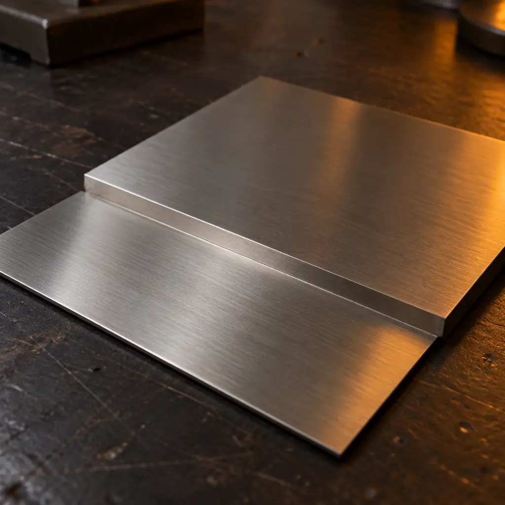
A step stencil is two stencils in one foil. The transition region carries no apertures and must be designed for the squeegee, not the print.
Reading Foil Thickness From the Cross-Section Report
The only reliable evidence that a supplier used the specified foil is the cross-section report on the first-article boards. It shows measured paste and solder thickness after reflow plus the measured foil thickness if the report includes a print-off check. Ask for both. A cross-section report that shows only the final fillet height cannot distinguish a thin gauge printed twice from a correct gauge printed once.
Three measurements in the report are diagnostic. Measured paste height before reflow should track foil thickness within 10 percent. Metal thickness after reflow should be close to that paste height minus flux loss, typically 60 to 70 percent of paste height in volume terms. Aperture wall film, visible as a thin paste line in the aperture outline in a print-off scan, indicates poor release and a gauge at or past its area ratio limit.
A supplier that cannot show paste height is likely sampling by eye. A supplier that reports a foil thickness but no aperture-level detail is quoting the spec on the travel sheet rather than measuring. Neither is fraudulent, but neither allows a buyer to verify the gauge was the one specified. Our first article inspection structure includes paste height and foil thickness as inspection line items for exactly this reason.
How Thickness Goes Into a Purchase Order
A purchase order that says "SMT stencil per customer specification" transfers no obligation. The specification should name the gauge per region and the release criteria that prove it was respected. Five lines cover it.
Named gauge and the aperture it was derived from
Specify foil thickness in microns and state the smallest aperture width on the design plus the calculated area ratio at that width. This converts a habit into a calculation and makes the number auditable.
Stepped regions with boundaries
If a step is used, name each region, the gauge in each, and the minimum clear distance around the step transition. Undefined boundaries produce squeegee trails that nobody owns.
Foil type and manufacturing method
Laser-cut stainless, electroformed nickel, or stainless with nano-coating. Each has different release behaviour and different lifecycle. Nano-coated foil can be specified with a minimum coating life in prints.
Paste height acceptance on first article
State the measured paste height range and the measurement method. Nominal plus or minus 10 percent is defensible for widths above 0.4 mm; below that, plus or minus 15 percent is realistic.
Report requirement
Require a print-off or cross-section image at the finest aperture alongside the first article report, plus the aperture list used to cut the foil. The aperture list is the fastest way to detect a supplier who re-used a stencil from another job.
Two contract points are worth adding. First, stencil ownership. If the tool was paid for by the buyer, the foil and its design file should be listed as buyer property at the end of the programme, along with any step patch data. The tooling and design file ownership guide covers how to word it. Second, remediation. Specify that if paste height at the finest aperture falls outside the agreed band on first article, the foil is remade at supplier cost before production, not adjusted by pressure or speed to compensate.
Where the volume shortfall shows up later rather than at print, the cost usually appears as a rework or field failure, and the question is who pays. The quality dispute resolution process is only useful if the stencil gauge and paste height were agreed in writing at the start.
A Decision Sequence You Can Run in Ten Minutes
Take the design, list every aperture by size, and find the smallest. Find the pad that needs the most paste volume, which is usually a through hole or a thermal pad. Calculate required volume for both. Then apply this sequence and stop at the first line that resolves the conflict.
Calculate area ratio at 120 micron for the finest aperture
If the result is 0.66 or better, 120 micron is a defensible base gauge and no step is needed for pitch. If it lands between 0.60 and 0.66, the choice is 100 micron or 120 micron with nano-coating, and the coating should be specified by name.
Check the largest pad's volume requirement at the finest-pitch gauge
If the largest pad is short by more than 20 percent at that gauge, a step is required. Short by less than 20 percent can often be covered by segmenting the pad into a higher aperture density.
Check pin-in-paste barrels separately
Barrel fill from print alone is rarely achievable. Record whether the intent is barrel fill from a second pass or from selective solder, and specify it. A joint specified as print-filled but actually wave-filled is a documentation defect.
Confirm step feasibility with the supplier's lead time
Laser-welded steps typically add two to four days. Electroformed stepped foils add more. If the programme cannot absorb that, the correct answer is a design change to the pad geometry, not a compromise gauge.
What we do on the line
For boards with a finest aperture of 0.30 mm or larger, we run 120 micron laser-cut stainless with nano-coating as the base gauge and check paste height at the finest aperture on every new tool. For 0.4 mm pitch with thermal pads, we go to a step from 100 to 150 micron and place the transition 3 mm clear of the nearest aperture. First-article reports include paste height at three aperture widths, not one average.
Thickness is the cheapest variable to get right and the most expensive to get wrong, because the error compounds across every board in the lot and only becomes visible after reflow. It belongs in the design review and in the purchase order, not in the printer operator's experience.
If you want the gauge checked against your actual aperture list rather than a rule of thumb, send the Gerber and paste layer with the board stack. We will return the area ratio calculation per aperture class and a thickness recommendation with the step regions marked.