

A thermal via array is the cheapest heat sink a designer can specify — a grid of plated holes under a power package that carries heat from the component's thermal pad down to an internal or back-side copper plane. It costs almost nothing in fabrication and it works. It also fails, quietly and repeatedly, in ways that never show up in a DFM report: the paste that should have filled the vias didn't, the vias wicked solder away from the joint, or the array sat on a plane that was fragmented into islands by a signal trace. This guide is for engineers and buyers specifying thermal vias on power, LED and motor-drive boards, and it covers the numbers that decide whether the array works: drill diameter, pitch, plating thickness, paste coverage, and the copper area on the far side.
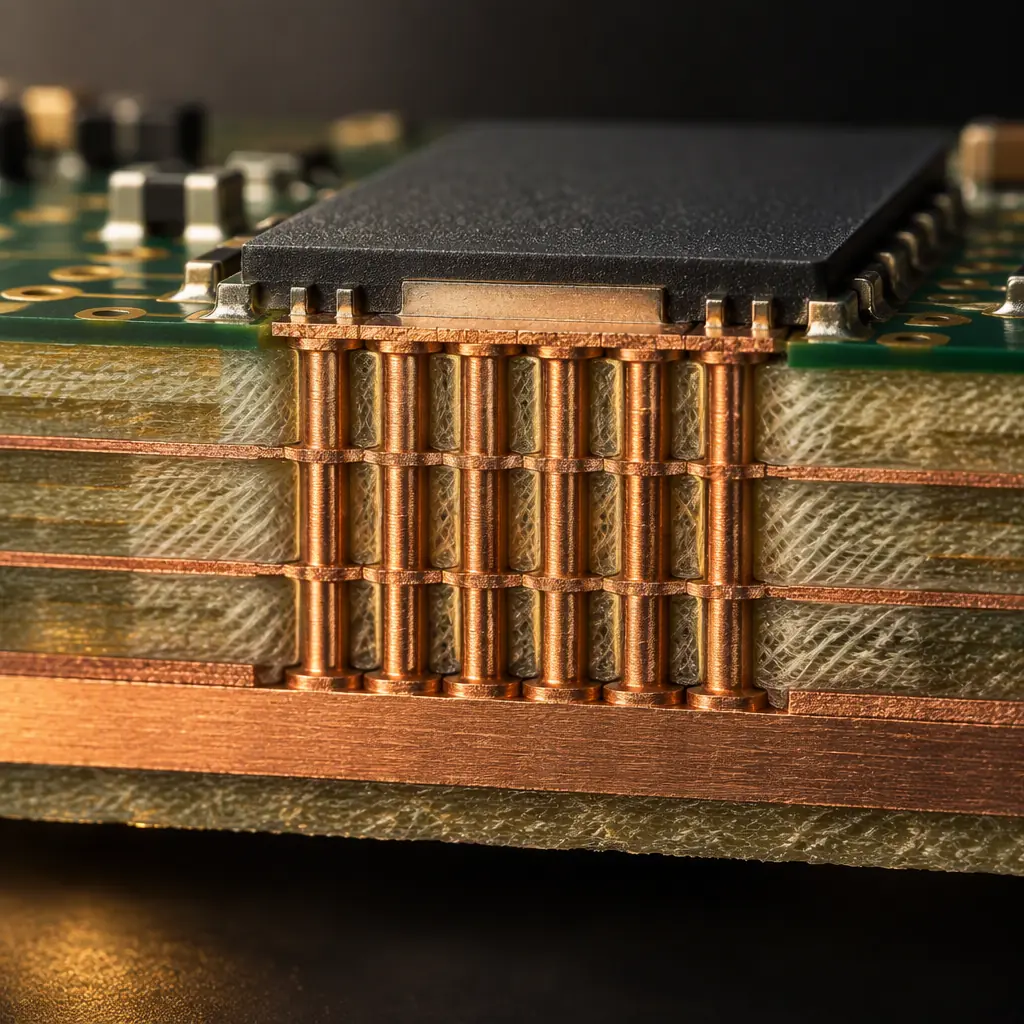
How Much Heat Can a Thermal Via Array Actually Move?
Start with the physics rather than the layout habit. A single 0.3 mm finished-hole copper barrel in 1.6 mm FR-4, with 25 µm of plating, carries a thermal resistance of roughly 100 K/W. That sounds terrible, and on its own it is. The reason arrays work is parallelism: twenty of those vias in parallel give about 5 K/W, which is comparable to a small bonded heat sink — and it costs nothing extra at fabrication.
Three variables dominate the result, and only the first is usually specified:
- Barrel copper thickness. Thermal resistance scales inversely with plating thickness. Moving from 20 µm to 25 µm of barrel copper is a 20% improvement; a filled and capped via (copper paste or resin plus plating) can be several times better because the fill conducts through the centre, not just the wall.
- Count, not size. Two 0.3 mm vias beat one 0.6 mm via. Doubling the drill diameter quadruples barrel area but only doubles the barrel circumference that actually conducts — while consuming four times the pad area. Dense small vias win.
- Board thickness. A 2.0 mm board has a 25% longer barrel than a 1.6 mm board and correspondingly higher resistance per via. Thick power boards need proportionally more vias or filled vias.
The practical specification that follows from this: 0.25–0.3 mm drill on a 0.8–1.0 mm pitch, which is a mature, low-risk fabrication window on any 2-layer or multilayer stack, gives the highest thermal conductance per unit of pad area. Going below 0.2 mm pushes you into laser-drilled microvias and a different cost tier; going above 0.4 mm starts to reduce count under a typical 5 × 5 mm QFN pad.
The Copper on the Far Side Is Half the Design
An array of vias that dumps heat into a plane the size of the package footprint is nearly useless. The plane on the receiving side is the actual heat spreader, and its area and continuity set the real thermal resistance. Two rules matter:
- Give the receiving plane at least 2–3× the package pad area, ideally the whole board on the back side of a small power board. A 5 × 5 mm pad feeding a 5 × 5 mm island gains almost nothing over no vias at all.
- Do not let signal traces fragment the plane. This is the most common layout failure on thermal arrays. A single trace crossing the receiving plane can cut it into two islands, roughly halving the effective spreader and doubling the temperature rise. Route signals on a different layer, or use a plane layer that is never used for routing.
If the bottom side of the assembly exposes the plane to air, adding a solder-mask opening there (or a bare copper window) lets convection and radiation help. Where the finished assembly slides into an aluminium housing, a gap pad between that copper window and the housing converts the whole product into the heat sink.
Thermal Relief Spokes vs Solid Connection — Get This Right
Thermal vias sit inside a pad that is also being soldered. If the pad is connected to a large plane with solid copper on every layer, the pad becomes a heat sink during reflow and the paste never reaches liquidus before the rest of the board. The joint is cold, dull, and often fails inspection or field life later.
The standard answer is a thermal relief: four spokes of 0.3–0.4 mm connecting the pad to the surrounding copper, rather than a full copper connection. The spokes throttle heat flow into the plane during reflow while still conducting in service. The exception is high-current pads, where the current-carrying requirement forces a solid connection — in that case the profile has to be extended (soak length, peak time above liquidus) to compensate, and the pad should be checked on first-article X-ray rather than assumed good.
Factory reality: on a QFN with an exposed pad, cold joints caused by solid plane connections account for a large share of the reflow defects we see on customer-supplied Gerbers. The fix is a 30-second layout change at design stage, or a profile change and a re-qualification at production stage. The first is free.

Do the Vias Need to Be Filled?
The question comes up on nearly every power board and the answer depends on what is on top of the via array:
| Condition on top of the array | Via requirement | Why |
|---|---|---|
| Recessed in a solder-mask-covered pad, no component | Tented, open barrels acceptable | No paste contact, so no wicking risk |
| Exposed thermal pad of QFN / DFN, paste printed over vias | Fill and cap, or tent from the top | Open barrels wick paste off the pad and cause voids |
| Under a BGA with a large ground pad | Fill and cap (copper or resin) | Solder wicking causes opens and shorts in the ball field |
| High-current path with 2 A or more per via | Copper fill preferred | Resin fill has negligible current capacity |
The cost difference is real but smaller than most buyers expect. On a 1.6 mm board, resin-filled and capped vias typically add a modest premium; VIP (copper-filled) processing adds more, because it requires plating and planarisation. Where the array sits under an exposed pad and paste is printed across it, filling is not optional. Open barrels pull paste off the pad during reflow by capillary action, leaving a starved joint and a voided thermal interface — and the void is invisible until X-ray.
What to Put in the Fabrication Notes
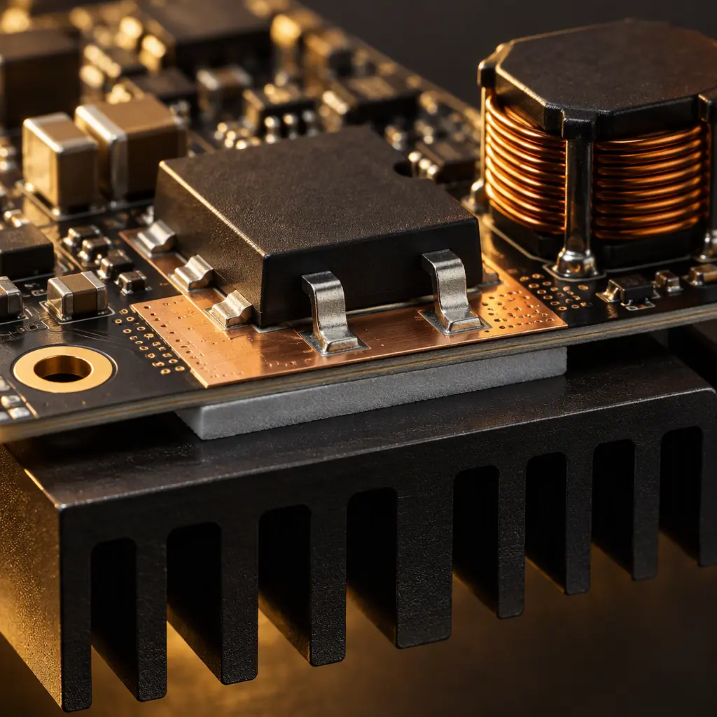
Thermal vias are one of the few features where a one-line note on the drawing removes almost all ambiguity. A complete specification looks like this:
- Drill diameter and finished hole size, with the pitch stated as a grid (for example "0.30 mm drill, 0.90 mm pitch, staggered").
- Barrel plating minimum — 25 µm is standard, and thicker plating is a direct thermal improvement.
- Fill requirement: tented-from-top, resin-filled and capped, or copper-filled and planarised.
- The receiving-layer copper minimum area, stated as a number, so the fabricator's CAM check can flag fragmentation.
- Whether the vias are on-grid with the component pad or on a separate mechanical array (the former is better for assembly).
Ambiguity here is expensive in both directions: a fabricator who guesses "tented" when the design needed "filled" produces boards that pass fabrication and fail assembly yield, and nobody discovers it until first-article X-ray.
Verification: How You Know the Array Works
Thermal vias are not visible after assembly, so verification has to be built in rather than inspected at the end. Three checks cover nearly all the risk:
- X-ray on first article. Look specifically at the void percentage on the exposed pad. Filled vias with a well-controlled print cycle land well under typical acceptance limits; open barrels show characteristic void patterns radiating from via locations.
- Thermal measurement on the first build. A thermocouple on the package top case, or an IR image of the running board, tells you whether the array plus plane is meeting the calculated rise. This is the only test that catches a fragmented receiving plane.
- Cross-section on a coupon. When the thermal design is marginal, a cross-section through the via field confirms barrel plating thickness and fill quality that X-ray cannot resolve.
The broader process context for how these checks fit into an assembly flow is covered in our PCB thermal management guide, and the interface between package and heat sink on the finished assembly is covered in thermal interface materials. Where the design needs more than vias can deliver, the metal-core PCB design rules explain when an insulated metal substrate replaces the via-and-plane approach entirely.
At Huaxing PCBA, thermal via fields are drilled, plated and filled on 32-layer capable fabrication lines in Shenzhen, with filled-and-capped via processing available as a standard option. We build to IPC-6012 Class 2 and 3 and assemble power and QFN packages across the 8 SMT lines. Send your stackup and pad drawing for a quote or ask an engineer to review the via array against your thermal budget before you release the design.