
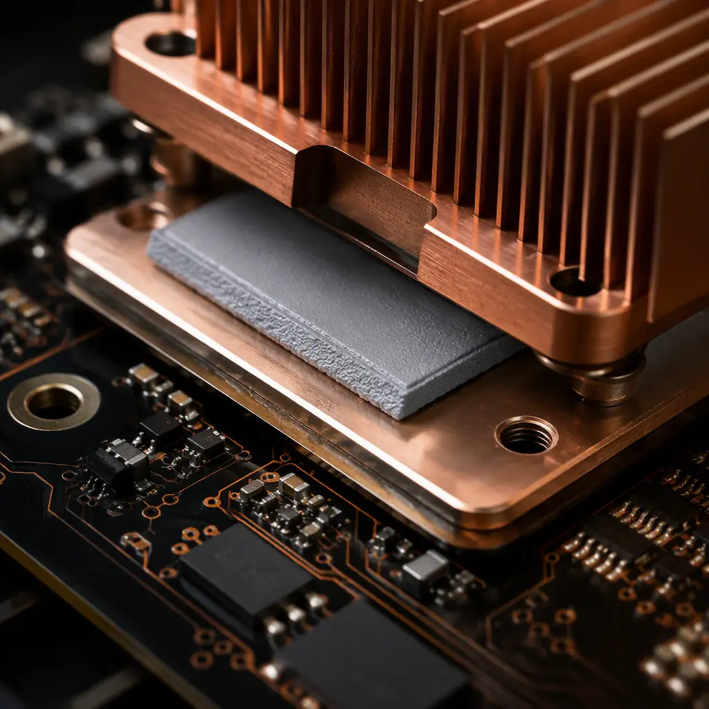
A thermal interface material fills the microscopic air gaps between two mating surfaces. Air is a terrible conductor at roughly 0.026 W/m·K, so an unaided contact between a power device and an aluminium heat sink is dominated by those air gaps and conducts far less than the metal itself would suggest. The TIM displaces that air with a conductive medium. A good TIM can reduce the thermal resistance of a power-device joint by a large factor, which is why the same board that runs at 110 °C junction with a thin gap pad may run at 75 °C with a properly applied pad of higher thermal conductivity. At Huaxing PCBA we build IATF 16949 and ISO 9001 certified boards with heavy copper, thermal vias and metal-core capability, and we assemble the power electronics that sit on top of them. See our thermal management guide for the board-side strategy.
This guide is specifically about the interface material between the board and the heat sink, the last few tenths of a millimetre that decide whether your design actually cools. There is no single best TIM; there is a best TIM for the joint gap, the pressure, the temperature range and the reliability requirement. We assemble governed high-power boards on 8 SMT lines with X-ray and AOI inspection, so we see both the application side and the test side of the equation.
The Four TIM Families and Where Each Fits
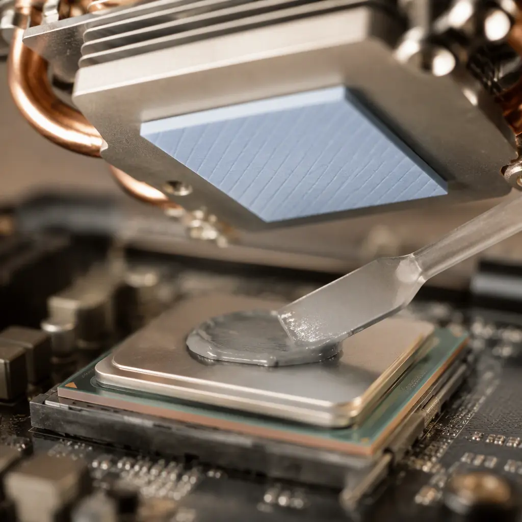
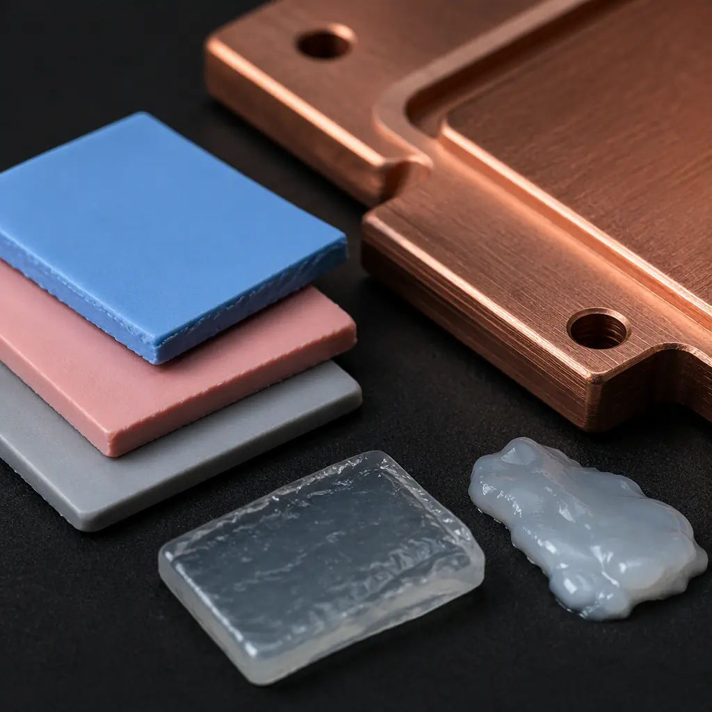
Broadly there are four types of thermal interface material a fab-and-assembly house will use, and each trades off thermal conductance, ease of assembly, reworkability and cost.
| Type | Typical conductivity | Gap tolerance | Best for |
|---|---|---|---|
| Thermal gap pad | 1.5–6+ W/m·K | 0.5–5 mm | Uneven parts, variable gaps, large contact patches |
| Thermal paste / grease | 2–6 W/m·K (to 12+ with fillers) | <0.25 mm, precise | Flat, high-pressure, well-machined joints |
| Phase-change material | 3–8 W/m·K when melted | Thin, conforms at operating temp | Reliability + min thickness, CPU/GPU style |
| Liquid metal | >20 W/m·K | Very thin | Extreme high power, fixed joints (rare on PCB) |
The first mistake is to chase the highest conductivity number. A 6 W/m·K gap pad that does not compress to fill the actual gap performs worse than a 3 W/m·K pad that does. The thermal resistance of the joint, not the material conductivity alone, is what your design sees. Our trace width & current capacity guide covers the copper side, but the joint resistance is a separate term in the same equation.
Reading a TIM Datasheet: What Actually Matters
Don't stop at conductivity, look at thermal resistance
Datasheets express performance as either conductivity (W/m·K) or thermal impedance (°C·cm²/W) at a given pressure and thickness. The impedance number is more honest because it includes the thickness and the surface-void penalty. Compare parts at the same thickness and pressure.
Match the pad to the real gap, not the nominal one
If your package sits 1 mm above the heat sink but the average gap over the foot is 1.6 mm because of board warpage, a 1 mm pad will not make contact everywhere. Specify the pad for the maximum gap, and account for board warpage.
Mind the pressure and the compliance
Gap pads have a compression curve. Not enough clamping pressure and the pad stays thick and poorly contacted; too much and you can crack the board or de-laminate a metal-core. Get the (psig) pressure point from the datasheet and the clamp design from the enclosure.
Gap Pads vs Paste: The Application Decision
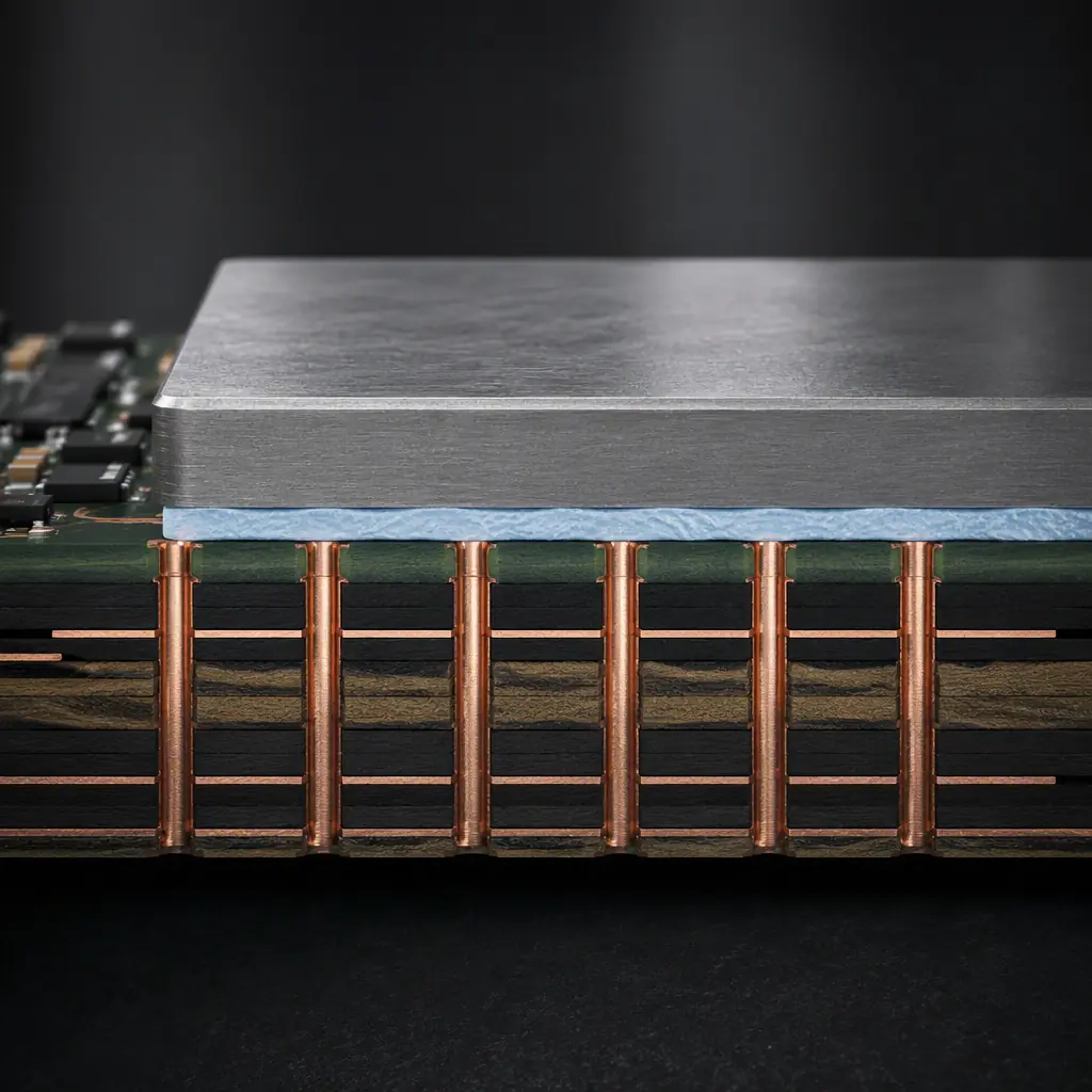
The choice between a pad and a paste is often decided by the assembly process, not the physics. Paste is cheap and conducts well, but it is a wet process that needs a controlled dispensing volume and it can smear onto components or migrate over time. A pad is a dry, easy-to-handle part that gives a repeatable thickness, is easier to inspect, and is simpler to rework. But it is more expensive and needs the higher compliance to fill a gap.
| Criterion | Gap pad | Thermal paste |
|---|---|---|
| Assembly | Dry, pre-cut, press-on | Dispense or stencil, then clamp |
| Thickness control | Excellent (fixed pad) | Variable (volume dependent) |
| Rework | Peel and replace | Clean and reapply |
| Cost | Higher per part | Lower |
| Gap range | Wide (0.5–5 mm) | Thin only |
For higher-volume, precisely-located power devices, many contract manufacturers prefer a pad because it removes the dispense-and-clamp variability from the line and is trivially inspectable with AOI. Our power electronics guide covers how the board itself is designed for these assemblies.
Phase-Change and Reliability for Vibration and Automotive
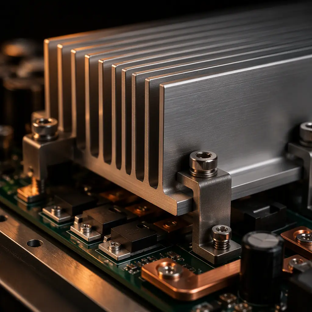
In an automotive, industrial or aerospace environment, a TIM that is easy to apply at room temperature is not automatically the one that survives ten years of vibration and thermal cycling. Phase-change materials are a strong compromise: they are solid and easy to handle and inspect at assembly, then soften and flow at operating temperature to fill the micro-gaps, giving thin, low-resistance, reliable joints. They are why phase-change is the default for a lot of automotive electronics.
Key Takeaway: In an automotive or harsh-environment program, specify the TIM against the reliability test, not just the datasheet. A paste that pumps out under vibration, or a pad that hardens and cracks after 1,000 thermal cycles, will fail your qualification even if it looked great on paper. Validate with the actual thermal cycling and vibration profile.
Outgassing, CTE and Material Compatibility
Two more selection criteria are easy to miss. The first is outgassing: a silicone-based TIM can release volatile compounds that fog lenses and contaminate optical or hermetically sealed assemblies, which is why aerospace and optics programs specify low-outgassing materials. The second is CTE and hardness: a material that is far harder than the board can transmit stress into the solder joints under thermal cycling, so match the compliance to the joint.
- Outgassing . Check the total mass loss and condensed volatiles (often to a NASA or ASTM standard) for optical and sealed assemblies. See our handling and cleanliness considerations.
- CTE & hardness . A soft, compliant gap pad protects BGA solder joints better than a hard paste on a rigid clamp during power cycling.
- Electrical & flammability . Confirm the pad is non-conductive (dielectric) and rated UL 94 V-0 if it carries any voltage near live parts.
- RoHS / REACH . As with all assembly materials, confirm restricted-substance compliance. See our RoHS compliance guide.
What a Contract Manufacturer Should Verify on the Line
The TIM application is a process step that can be inspected, and a good assembler will give you evidence, not assumptions.
Verify pad placement and coverage
A gap pad that is cut to the wrong size, placed off-centre, or has a liner not fully removed leaves a cold spot. A placement jig plus an inspection step (AOI or camera) confirms the pad covers the full heat-source footprint.
Control the clamp torque
For a screwed heat-sink clamp, torque is the pressure. Under-torqued joints leave a gap; over-torqued joints crack the board or a metal-core. Give the assembly a defined torque spec and a documented tightening procedure.
Sample thermal test on the reference unit
Measure junction or case temperature under load on a reference assembly, and compare against the thermal model. This closes the loop and tells you whether the TIM is actually performing. Our testing methods guide covers the measurement options.
Summary: The TIM Is Part of the Design, Not an Afterthought
Pick the thermal interface material the way you pick any other load-bearing part of the thermal path. Read the thermal resistance at the operating pressure and thickness, match the pad to the real (warped) gap, choose between paste and a pad from the assembly and rework standpoint, use phase-change where vibration and reliability demand it, and check outgassing, CTE, flammability and RoHS. Then have your assembler prove it with placement, torque and thermal checks.
At Huaxing PCBA we build IATF 16949 and ISO 9001 certified boards with heavy copper, metal-core, thermal vias and up to 32 layers, and we assemble and box-build the power electronics that use them, on 8 SMT lines with 8M placements/day and X-ray and AOI inspection. We can review your thermal path and tell you what will actually cool your device before you commit. Get a quote or ask our engineering team about your thermal interface.
