
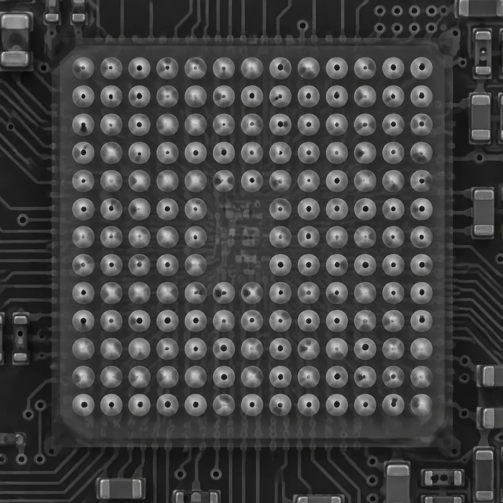
A void is a pocket of gas trapped inside a solder joint. It forms during reflow when flux volatiles, moisture, or entrapped air cannot escape before the solder solidifies, leaving a bubble frozen in the metal. Under x-ray, voids appear as bright-edged dark circles inside the joint. They are present to some degree in almost every reflowed joint, which is why the question is never "are there voids" but "how much voiding is acceptable for this joint, in this location, on this product." That question has a defined answer, and the answer is not the same for a signal ball on a BGA as it is for the thermal pad of a power device.
This guide covers what causes solder voids, how they are measured, what the IPC-7095 standard actually specifies for BGA and area-array joints, how thermal-pad voiding is judged differently, and how to write a void specification that a fabricator can hold to and an inspector can verify. At Huaxing PCBA we inspect to IPC-7095 criteria across 8 SMT lines under IATF 16949 and ISO 9001, and we state the void limit for critical joints on the inspection plan for every order.
What Actually Causes a Solder Void
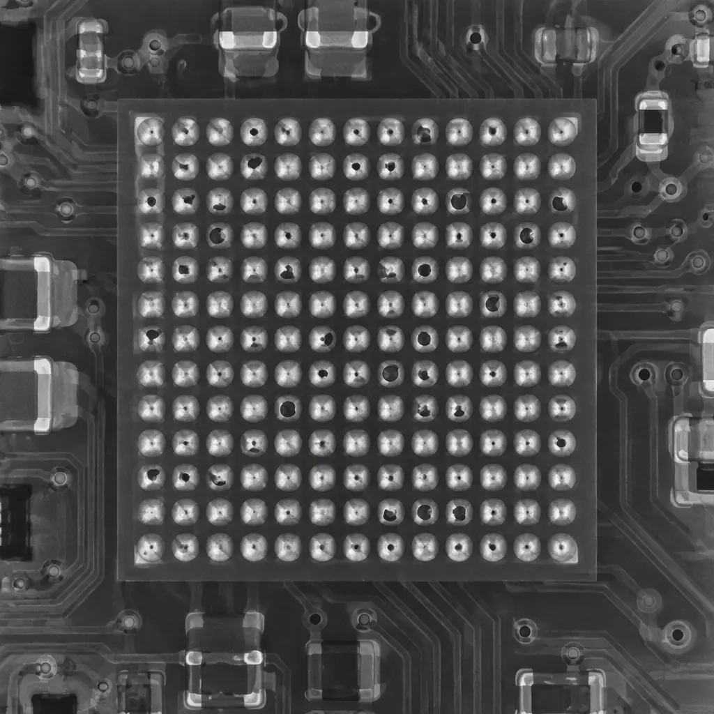
Voids have a small number of root causes, and identifying which one applies is the difference between a fixable process issue and an unavoidable material property.
Flux volatiles and outgassing. The most common cause. Solder paste carries flux, and that flux contains solvents that vaporise during the reflow ramp. If the paste is heated too quickly at the start of the profile, the volatiles evolve faster than they can escape through the still-liquid solder, and some fraction is trapped. A slower, longer soak — often called a soak profile — lets the volatiles escape before the solder fully melts, and reliably reduces voiding. This is the first lever to pull and often the only one needed.
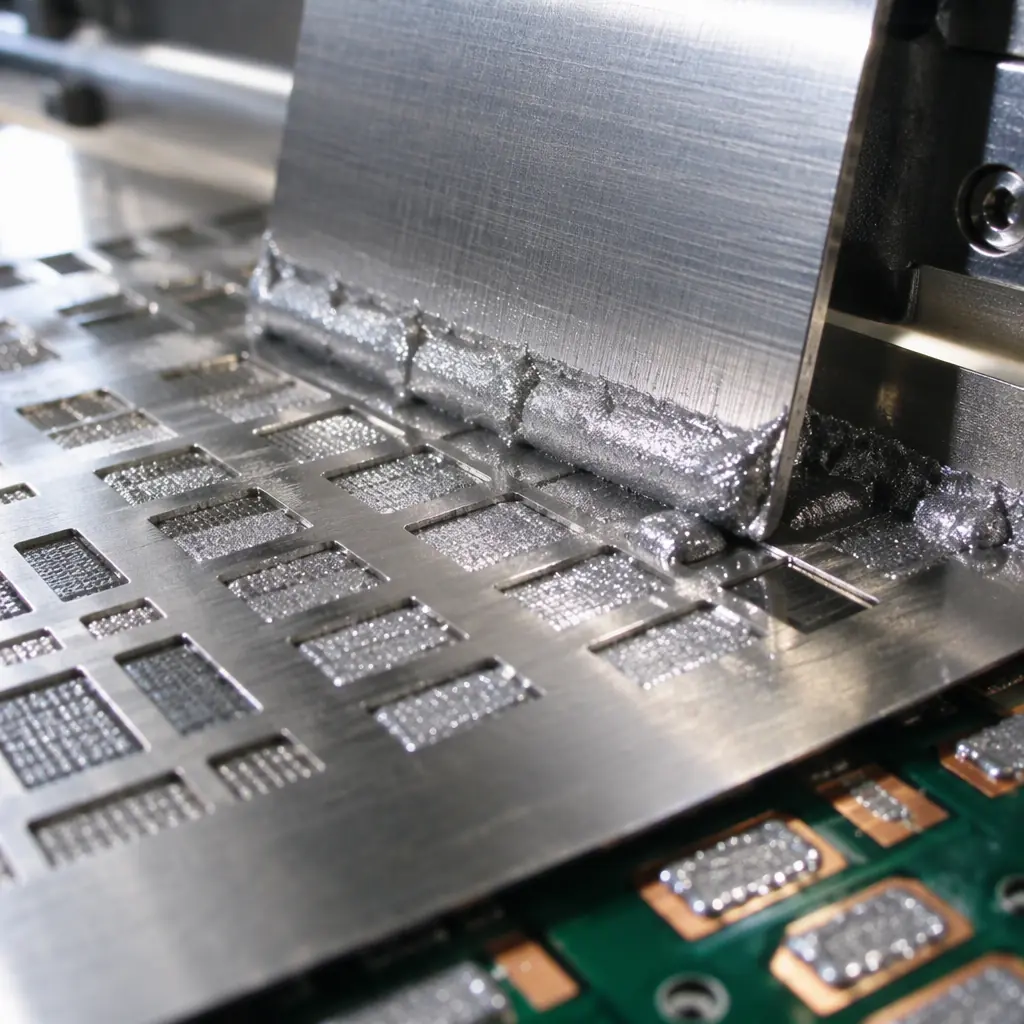
Entrapped air from paste deposition. Solder paste is about half metal by volume and half flux by volume. That flux is not all volatile; some remains as residue, but the paste as printed occupies a volume far larger than the final joint. At reflow the paste collapses to roughly half its printed height as the flux escapes. If the paste print has a centre dip, a poor release from the stencil, or an air pocket from a bad stencil aperture, that geometry can seal off a gas path and produce voids larger than the baseline.
Oxidation and surface contamination. Oxidised pads or component terminations, or contamination on the copper, change how the molten solder wets. Poor wetting can leave voids at the pad interface — the so-called interfacial void — which is more damaging than a void floating in the bulk of the joint because it reduces the actual bonded area. Clean surfaces and the correct flux activity reduce these.
Moisture and via outgassing. If a PCB has absorbed moisture before assembly and is not adequately baked, that moisture flashes to steam at reflow temperature. Where the joint sits over a via or a plated hole, the steam escapes through the joint and leaves a void. Likewise, the vapour escaping from an unfilled via-in-pad can produce a characteristic void pattern. Baking per J-STD-033 before reflow, and filling or capping vias under thermal pads, removes this cause.
How Voiding Is Measured
Before any acceptance limit means anything, the measurement has to be defined, because the same joint can report very different void percentages depending on how the number is calculated.
The standard metric is the total void area as a percentage of the joint area, measured on a two-dimensional x-ray projection. The inspector sums the areas of all detectable voids within the joint and divides by the joint's total projected area. Two details change the result and must be agreed: the minimum void size that is counted, and whether the joint area is the ball footprint or the full ball projection. A specification that does not fix these two parameters is not enforceable, because a lenient inspector can exclude small voids and inflate the joint area to pass a joint a strict inspector would fail.
Three measurement approaches are in common use:
| Method | How It Works | Use |
|---|---|---|
| Manual 2D x-ray | Operator views the joint and estimates void area against the joint | Rapid screening; subjective, best for obvious failures |
| Automated 2D x-ray software | Software thresholds grey levels and computes void area automatically | Repeatable, quantitative; the practical standard for acceptance |
| 3D CT (computed tomography) | Reconstructs void volume, not just projected area | Failure analysis and process development; too slow for production |
For production acceptance, automated 2D x-ray software is the practical choice: it removes operator judgement and produces a number that can be trended. 3D CT is reserved for failure analysis and for validating a process, because it reveals void location in three dimensions and will catch an interfacial void that a 2D projection can hide against the joint outline.
IPC-7095 — The Void Criteria by Class
IPC-7095, the standard for design and assembly of BGA and other area-array packages, is the reference that governs void acceptance for ball-grid joints. It does not set a single number for the whole industry; it recognises that voiding means different things depending on where the void is and how much of the joint's load path it interrupts.
For BGA balls, the standard's widely applied engineering guidance is that the total void area should generally not exceed approximately 25% of the ball area for a standard joint, with the critical caveat that voids must not be concentrated in a way that disrupts the bond between the ball and the pad. A void sitting centrally in the bulk of the ball, surrounded by bonded metal, is structurally very different from a void at the interface, which directly reduces the bonded area. The class-based stringency then scales: Class 3 high-reliability product is inspected more strictly and interfacial voiding is treated far more seriously than in Class 2 commercial product, where the same total percentage may be acceptable if the void is in the bulk.
Key Takeaway: The number that matters is not the total void percentage alone but where the void sits. Up to about 25% total area in the bulk of a BGA ball is generally tolerated for standard product; the same void concentrated at the pad interface is a concern even at low percentages because it reduces the bonded area. Always specify both a total limit and a location rule.
Two further points are frequently missed. First, the standard treats voiding in terms of process capability and the joint's function rather than a single pass-fail line, so a fabricator with a stable process can justify accepting higher voiding where a low-power joint's electrical and thermal performance is unaffected. Second, the criteria apply to the finished joint after reflow and, for a second-side or double-reflow process, must be evaluated after the final reflow that the joint experiences — a joint reflowed twice can show different voiding than the same joint reflowed once.
Thermal Pads Are Judged Differently
Voiding under a thermal pad — the large exposed pad on a QFN, LGA, or power device — follows a different logic because the joint's job is different. A thermal pad carries heat away from the die, and heat flows across the whole pad area rather than through a single signal path. A void in a signal ball interrupts a conductor; a void in a thermal pad reduces the effective heat-transfer area.
Because of this, thermal-pad voiding is assessed against the pad area rather than a ball area, and the acceptance thresholds are tighter for thermally critical devices. Many assembly specifications cap centre-pad voiding at a much lower percentage than a BGA ball — commonly in the range of 10% to 25% of the pad area, with the exact figure set by the device manufacturer's thermal requirement. The practical approach is to take the void limit from the component datasheet or the customer's thermal analysis rather than to apply a generic BGA number to a thermal pad.
The mitigation for thermal-pad voids is also different: because these pads are often large and flat, the paste print design does. Splitting the paste into a grid or windowpane pattern rather than a single solid deposit gives the volatiles a network of escape channels and dramatically reduces voiding. Our guide to QFN and LGA soldering covers the stencil and paste design for leadless thermal pads in detail, and the broader AOI, X-ray and SPI inspection guide explains where x-ray fits in the inspection flow.

Reducing Voiding at the Process
Voiding is a process outcome, and the levers that control it are well established. When a void level is out of specification, these are the variables to work in order.
Adjust the reflow profile before changing anything else
A longer soak and a slower ramp let flux volatiles escape before the solder fully melts. This single change resolves the majority of ordinary voiding and costs nothing but profile time.
Redesign the paste deposit for large pads
Split a large thermal-pad or ground-pad deposit into a grid, windowpane, or multiple smaller apertures so the flux has escape channels. Solid deposits over large areas trap gas.
Bake moisture out and cap vias
Bake per J-STD-033 before reflow so absorbed moisture does not flash to steam inside the joint, and fill or cap vias that sit under thermal pads so the via does not vent through the joint.
Control paste volume and stencil release
Voiding correlates with paste volume variation and poor stencil release. Confirming paste volume with SPI and improving the aperture design reduces both the void level and its unit-to-unit spread.
Writing a Void Spec That Holds
A void specification is only useful if both parties measure the same thing. The following elements make it enforceable.
State the measurement method — automated 2D x-ray with a defined minimum detectable void size — so that the number is reproducible. State the total void-area limit as a percentage of the relevant area, and say explicitly whether the relevant area is the ball footprint or the pad area. Add a location rule: for BGA, no interfacial voiding in the bonded region for Class 3; for thermal pads, the limit taken from the device thermal requirement. Set the sample plan — how many joints, from how many boards, at what frequency — because voiding varies board to board. Finally, state the remedy when a joint exceeds the limit, so the acceptance decision is made once, in the specification, rather than re-argued at each shipment.
At Huaxing PCBA we inspect to IPC-7095 criteria across 8 SMT lines under IATF 16949 and ISO 9001, and we put the void limit for critical joints on the inspection plan before production. Send your Gerber and BOM with the critical joints marked and we will confirm the void specification and return a quote with the inspection plan inside 24 hours, or talk to our engineering team about a voiding problem on a current assembly.
