
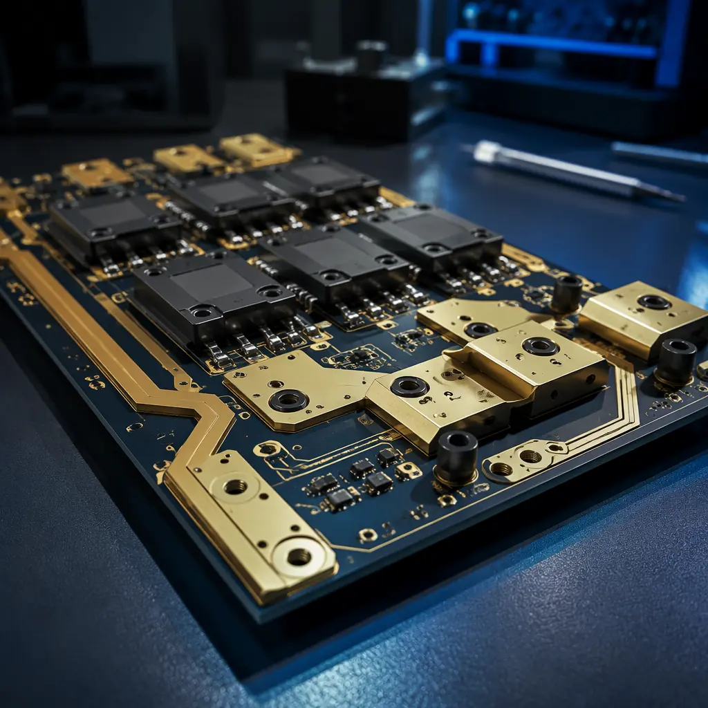
Every EV charger, solar inverter, and industrial motor drive on the market today depends on one component that rarely gets the attention it deserves: the power electronics PCB. This isn't a standard FR-4 board running 3.3V logic signals. Power PCBs carry 50 to 200 amps through copper planes, dissipate hundreds of watts of heat, and must survive thermal cycling from -40°C to 150°C for a decade, all while maintaining dielectric integrity at 1,000V or more.
At Huaxing PCBA, we manufacture power electronics PCBs across 8 SMT lines with copper weights up to 6oz and substrates including aluminum IMS, ceramic (Al₂O₃/AlN), and high-Tg FR-4 rated to 180°C. Our IATF 16949-certified facility processes over 800 million solder joints daily, and power electronics represent one of our fastest-growing segments, driven by global electrification across automotive, industrial, and renewable energy markets.
Thermal Management: The Defining Challenge of Power Electronics PCBs
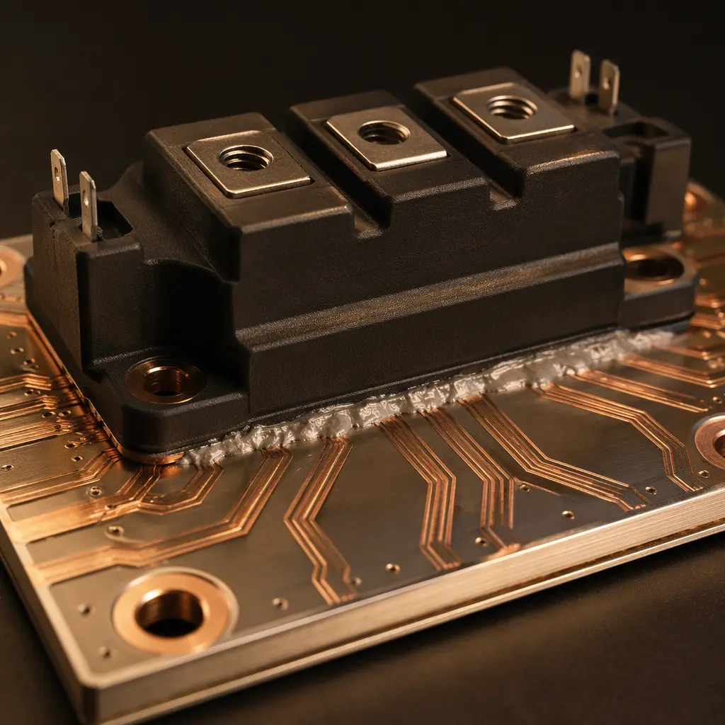
A standard PCB dissipates heat through convection and radiation from its surface. Adequate for logic boards pulling 5W. A power electronics PCB handling 500W or more needs a fundamentally different approach. The failure mode is well understood: every 10°C rise in junction temperature halves the expected lifetime of power semiconductors. Your substrate choice, copper weight, and via strategy don't just affect performance, they determine whether the board survives year three.
Insulated Metal Substrate (IMS / Aluminum-Core PCB)
IMS bonds the copper circuit layer directly to an aluminum or copper base plate through a thin dielectric layer (typically 75-150μm). This eliminates the thermal bottleneck of FR-4 and achieves thermal conductivity of 1.0-3.0 W/m·K, roughly 5-10× better than standard FR-4 (0.25 W/m·K). For LED drivers, DC-DC converters, and single-layer power modules, IMS is the cost-effective default. See our metal-core PCB guide for substrate selection by power level.
Heavy Copper with Thermal Via Arrays
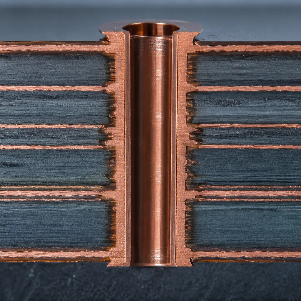
For multilayer designs where IMS isn't practical (signal layers + power planes in one stackup), heavy copper, 4oz to 6oz on outer layers, 2oz to 4oz on inner planes, paired with dense thermal via arrays is the standard solution. Thermal vias (plated through-holes filled with conductive epoxy or left unfilled) create vertical heat paths from hot components to a heatsink on the opposite side. A single 0.3mm filled thermal via conducts roughly 0.25 W/K; a 10×10 array under a TO-247 package can move 25W directly to the heatsink. Our heavy copper PCB manufacturing guide covers the trade-offs between copper weight, etch resolution, and cost.
Ceramic Substrates for Extreme Environments
Alumina (Al₂O₃, 96%) and aluminum nitride (AlN) substrates deliver thermal conductivity of 24 W/m·K and 170 W/m·K respectively, orders of magnitude beyond any organic laminate. Ceramic PCBs use direct-bonded copper (DBC) or direct-plated copper (DPC) processes to form circuits on the ceramic carrier. They're the standard for SiC MOSFET and GaN HEMT modules in traction inverters, where junction temperatures routinely exceed 175°C. The trade-off: ceramic is brittle, limited to smaller panel sizes (typically 140×190mm max at our facility), and 3-5× the cost of IMS per square inch.
Procurement Reality: The substrate decision has the single largest impact on both BOM cost and field reliability. An IMS board that saves $2/unit but fails at 18 months in a solar inverter installation (where replacement labor costs $500+) is not a savings, it's a liability. Always specify substrate type explicitly in your RFQ rather than letting the manufacturer default to FR-4.
High-Current Copper Design: Trace Width, Thickness, and Creepage
High-current PCB design is a three-way negotiation between copper weight, trace width, and temperature rise. The IPC-2152 standard replaced the older IPC-2221 charts with more accurate models that account for copper plane proximity and multi-layer thermal coupling, but the procurement engineer doesn't need to run the simulation. What you need is the checklist of what to ask for.
| Copper Weight | Trace Width for 50A (10°C rise) | Typical Application | Min Etch Resolution |
|---|---|---|---|
| 1oz (35μm) | ~50mm (external) | Signal, logic | 3/3mil |
| 2oz (70μm) | ~25mm | Medium power, POL converters | 4/4mil |
| 4oz (140μm) | ~12mm | DC-DC, motor drives | 6/6mil |
| 6oz (210μm) | ~8mm | Traction inverters, welders | 8/8mil |
| Busbar (2mm+) | N/A, external bar | 200A+ distribution | Mech. assembly |
Two practical rules for procurement specifications: first, always specify both base copper and plated copper, the plating step adds 20-25μm to outer layers, which affects both current capacity and impedance. Second, power traces on inner layers run hotter than outer layers (no direct convection cooling), requiring a 15-20% derating for the same cross-sectional area. When in doubt, run the board at 4oz inner / 6oz outer. The cost delta is under 10% for most designs but the thermal margin is substantial.
Creepage and Clearance for High-Voltage Sections
Power electronics PCBs frequently operate at 400V (EV bus), 800V (next-gen EV), or 1,000V+ (solar string inverters). IPC-2221 specifies 0.6mm clearance for 100V and 3.2mm for 500V on uncoated external conductors. For 1,000V designs, expect to maintain at least 6mm between high-voltage and low-voltage domains. Conformal coating, which our facility applies in-line after assembly, effectively doubles the withstand voltage for a given spacing. Our conformal coating guide details the coating types and application methods for high-voltage PCBs.
Substrate Selection: Matching Materials to Switching Frequency and Voltage
The substrate does more than carry heat. At the switching frequencies of modern power semiconductors, 20kHz for IGBTs, 100-500kHz for SiC MOSFETs, and 1MHz+ for GaN HEMTs, the laminate's dielectric constant (Dk), dissipation factor (Df), and comparative tracking index (CTI) become critical design parameters. Choosing the wrong material produces a board that works on the bench but fails EMC compliance testing.
| Material | Tg (°C) | Thermal Cond. (W/m·K) | Dk @ 1MHz | CTI (V) | Best For |
|---|---|---|---|---|---|
| Standard FR-4 | 130-140 | 0.25 | 4.5-4.7 | 175-225 | Logic, sub-48V |
| High-Tg FR-4 | 170-180 | 0.3-0.4 | 4.3-4.5 | 200-250 | Industrial drives, 48-400V |
| Aluminum IMS | 130 (dielectric) | 1.0-3.0 | 4.0-6.0 | , | LED, DC-DC, single-layer |
| Rogers 4350B | >280 | 0.69 | 3.48 ±0.05 | >600 | RF power, GaN, 500kHz+ |
| Alumina (96% Al₂O₃) | N/A | 24 | 9.8 | >600 | SiC modules, >400V |
| AlN Ceramic | N/A | 170 | 8.8 | >600 | High-power SiC, >175°C Tj |
For the procurement engineer, two specifications matter most: CTI and Dk stability. A CTI below 200V means the PCB surface can form conductive tracks under contamination and voltage stress. A failure mechanism that takes months to appear in the field. For outdoor applications (solar, EV charging), specify CTI ≥ 400V minimum. Our PCB materials selection guide covers the full substrate landscape with cost comparisons.
Manufacturing Quality Control for Power PCBs
Power electronics PCB failures are disproportionately expensive. A delamination defect in a consumer router is a warranty return. The same defect in a traction inverter stops a $40,000 vehicle. The manufacturing QC requirements for power PCBs go well beyond standard IPC Class 2. And procurement engineers should know which tests to specify in their purchase order.
High-Pot (HiPot) Dielectric Withstand Testing
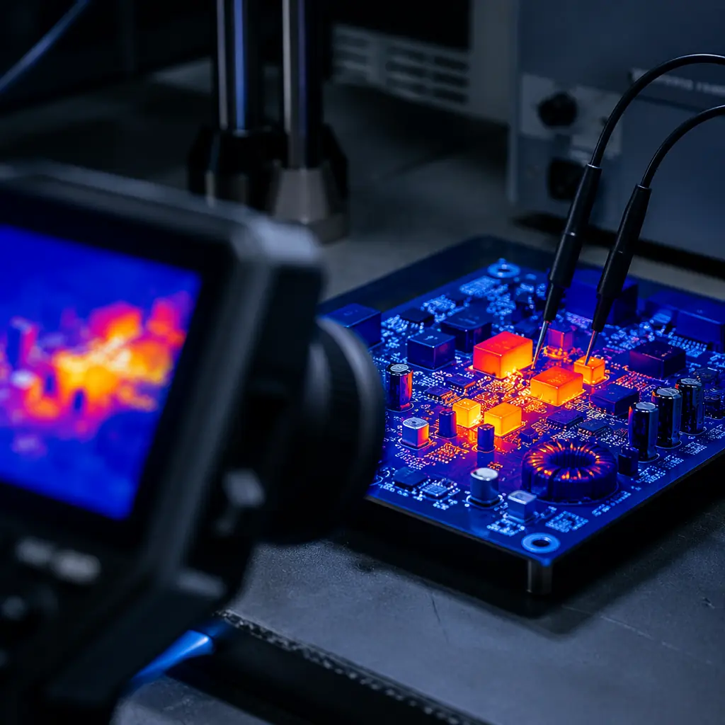
Every power PCB leaving our facility undergoes hi-pot testing: applying 1,500V DC (or 2× rated voltage + 1,000V) between isolated domains for 60 seconds while measuring leakage current. A board that passes at 500V but arcs at 1,200V has a latent manufacturing defect, incomplete etching between planes, insufficient dielectric thickness, or contamination. For automotive applications (IATF 16949), hi-pot results are archived per serial number for full traceability. Our PCB testing methods overview covers the complete electrical verification workflow.
Thermal Cycling and Thermal Shock Testing
The most common failure mode in power PCBs is barrel cracking, the copper plating inside vias fractures after repeated thermal expansion cycles. Plated through-holes expand at 17 ppm/°C (copper) while the surrounding FR-4 expands at 14 ppm/°C (XY) and 70 ppm/°C (Z-axis). Over 1,000 cycles from -40°C to +125°C, this CTE mismatch accumulates stress that eventually cracks via barrels. We test production samples to IPC-TM-650 2.6.7.1 (thermal shock) and 2.6.7.3 (thermal cycling), with cross-section analysis at 200× magnification to verify barrel integrity. Boards destined for automotive or renewable energy applications must pass 1,000 cycles with ≤10% resistance change.
Partial Discharge Testing for Medium-Voltage Boards
Once operating voltages exceed 700V, partial discharge (PD) becomes a real failure mechanism. Tiny voids in the laminate, incomplete resin fill in vias, or sharp copper edges create localized electric field concentrations where corona discharges can initiate. These micro-arcs erode dielectric material slowly, the board might pass initial hi-pot but fail after 6-12 months of continuous operation. For designs above 700V, specify PD testing per IEC 60270 with an inception voltage ≥ 1.5× rated operating voltage. This test requires specialized equipment that not every PCB shop has, confirm your supplier's PD capability before placing the order.
Factory Reality: A power PCB that passes electrical test at 25°C can still fail after 6 months in a rooftop solar inverter. The failure isn't in the copper, it's in the dielectric. Always request thermal cycle test reports for the specific stackup you're buying, not a generic qualification report for the material alone. The laminate datasheet tells you material properties; the stackup qualification tells you whether those materials work together under YOUR thermal conditions.
How to Specify Power Electronics PCBs: A Procurement Engineer's Checklist
Most RFQs for power PCBs are underspecified. The engineer who designed the board knows what they need; the procurement team translating that design into a purchase order often omits the critical parameters that distinguish a qualified supplier from a price-only bidder. Here is the minimum specification set every power PCB RFQ should include.
Substrate: material, thickness, copper weight (base + plated), Tg, CTI
Don't write "FR-4." Write "High-Tg FR-4, Tg ≥ 170°C, CTI ≥ 400V, 1.6mm thickness, 4oz outer / 2oz inner." The difference between the two specs is the difference between a board that works and a board that works for 10 years.
Dielectric withstand voltage: VDC, duration, acceptance criteria
Example: "1,500 VDC for 60 seconds between primary and secondary, leakage < 1mA." Without this, the supplier applies whatever voltage their standard QC checklist says — which may be 500V for a board that needs to handle 800V.
IPC class: Class 2 vs Class 3, and what that means for your specific board
IPC Class 3 reduces acceptable barrel voids from 10% to 5% of barrel length, mandates 360° wrap plating on vias, and tightens annular ring requirements. For automotive, medical, and aerospace power electronics, Class 3 is the default. See our IPC Class 2 vs Class 3 comparison for the full acceptance criteria differences.
Thermal cycle qualification: cycle count, temperature range, acceptance delta-R
Example: "500 cycles, -40°C to +125°C, 15-minute dwell, ≤ 10% resistance change per IPC-TM-650 2.6.7.1." For EV traction applications, specify 1,000 cycles minimum.
Partial discharge: inception voltage and test standard
Required above 700V operating voltage. "PD inception ≥ 1,050 VDC, IEC 60270." Not every supplier has PD test capability. This spec alone filters out shops that can't handle medium-voltage designs.
Conformal coating: type, thickness, coverage areas
For outdoor and high-humidity applications, coating isn't optional. Specify acrylic (AR), silicone (SR), or parylene (XY) with target thickness (typically 25-75μm for acrylic, 50-200μm for silicone) and masked areas (connectors, test points).
Power Electronics PCB Applications Across Industries
The power PCB requirements vary significantly by end application. A solar inverter PCB and an EV onboard charger PCB both handle kilowatts. But their failure modes, regulatory requirements, and cost constraints are completely different.
EV Chargers and Traction Inverters
Operating at 400-800V bus voltage with 100-300A phase currents, these boards use ceramic DBC substrates for the power stage and high-Tg FR-4 for control circuitry: often combined in a single assembly through press-fit or soldered interconnects. IATF 16949 certification is non-negotiable. Our automotive PCB requirements guide covers the full qualification framework, including PPAP Level 3 and IMDS material declarations.
Solar Inverters and Energy Storage
String inverters (1,000-1,500V DC input, 3-phase AC output) and hybrid inverters with battery connections demand the highest CTI ratings and thick copper (4-6oz). Outdoor installation means conformal coating is mandatory. These boards see the full temperature swing from -30°C winter nights to +70°C enclosure interiors in summer, thermal cycle qualification isn't optional. Our new energy PCB manufacturing guide addresses the specific challenges of photovoltaic and energy storage power electronics.
Industrial Motor Drives and Servo Amplifiers
Industrial VFDs and servo drives operate at lower voltages (380-480V AC) but face the harshest environments: vibration, conductive dust, and 24/7 duty cycles. Aluminum IMS with heavy copper circuitry is the dominant construction for drives up to 15kW; above that, separate power modules with laminated busbars become more practical than single-board solutions. These boards must pass industrial control PCB qualification with extended burn-in testing, 48 hours at elevated temperature and full load before shipment.
Getting Your Power Electronics PCB Project Started
Power electronics PCB manufacturing sits at the intersection of materials science, thermal engineering, and precision fabrication. The right supplier doesn't just etch copper and drill holes. They understand the physics of dielectric breakdown, the metallurgy of plated vias under thermal stress, and the statistical quality control needed to deliver zero-field-failure production runs.
At Huaxing PCBA, we manufacture power electronics PCBs across the full technology spectrum, from single-sided aluminum IMS for LED drivers to 6-layer heavy copper with Rogers high-frequency laminates for SiC-based traction inverters. Our controlled impedance capability maintains ±5% tolerance for gate drive circuits where picosecond timing margins determine switching loss, and our certifications portfolio covers IATF 16949, ISO 9001, ISO 14001, and UL (E354321), the full qualification package automotive and industrial OEMs require.
Send your Gerber files and stackup requirements to our engineering team for a same-day DFM review. We'll evaluate your design against IPC Class 3 criteria at no charge, identify thermal and manufacturability risks before you commit to production, and return a detailed quotation within 24 hours: including substrate options, copper weight recommendations, and qualification test plans tailored to your application.
