
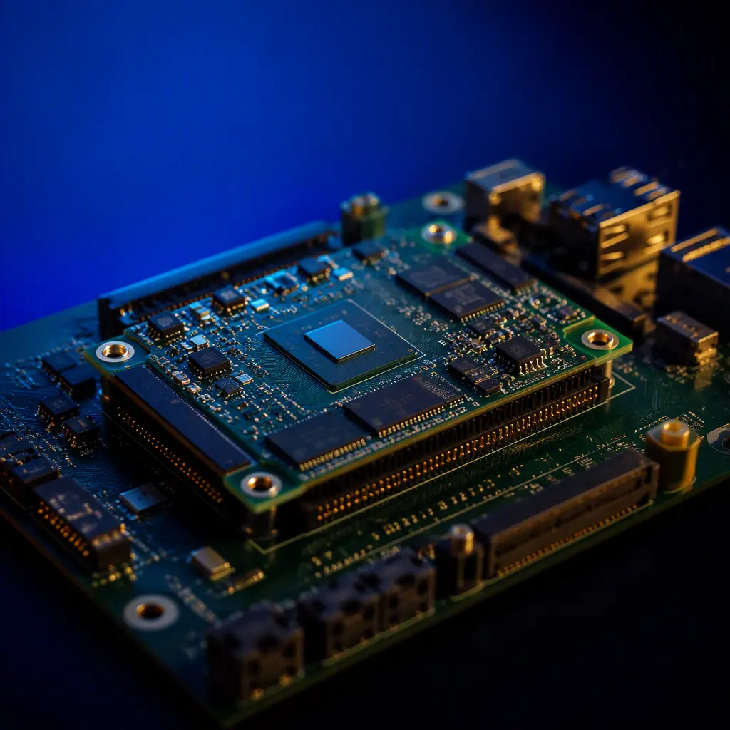
System-on-Module (SoM) development has become the dominant strategy for industrial, medical, and IoT products that need serious computing without a multi-million-dollar processor design program. You buy a module that packages the CPU, memory, and power management, then design a carrier board that provides the power input, connectors, and I/O your product actually needs. The trade-off is that the carrier board is no longer a simple board — it carries PCIe, USB 3.x, MIPI, and Gigabit Ethernet through a dense connector, feeds a half-dozen power rails, and has to stay manufacturable at volume. That is exactly the middle ground where a good manufacturing partner saves a project.
Huaxing PCBA builds carrier boards for compute modules across industrial automation, medical, and edge-AI applications — high-layer-count stackups, controlled impedance to ±5%, press-fit and SMT connector assembly, X-ray inspection of fine-pitch connectors, and full box-build integration. This guide covers the connector choice, the power tree, high-speed routing, thermal/mechanical integration, and the DFM requirements to put on the drawing.
SoM vs Custom Processor Board: When a Carrier Makes Sense
The first decision is architectural: integrate the processor yourself, or mount a module on a carrier. The answer shapes the whole program, from NRE to supply chain.
| Factor | Custom Processor Board | SoM + Carrier Board |
|---|---|---|
| Hardware NRE | High — CPU, memory, PMIC design | Low — module vendor did the hard part |
| Time to first prototype | 6-12 months | 4-8 weeks for the carrier |
| Processor upgrade path | Full redesign | Swap the module, keep the carrier |
| Unit BOM cost | Lower at very high volume | Module premium ($20-150) |
| Design risk | DDR routing, PMIC, boot bring-up | Module vendor already validated it |
| Best volume range | 100k+/year, long lifecycle | 1k-100k/year, fast-changing features |
The crossover point is usually around 50k-100k units per year: below it, the module premium is cheaper than the engineering and risk of a custom processor design; above it, the BOM savings of integration start to win. For most industrial and medical products — which ship in the thousands, not millions — the SoM approach is the rational choice, and the carrier board becomes the product.
Key Takeaway: A carrier board moves your product's risk from "will the DDR boot?" to "does the board feed power and route I/O correctly?" — a much smaller, more manageable engineering problem, and one where DFM experience pays off immediately.
Choosing the Module Form Factor and Connector
The module ecosystem spans hobbyist-friendly boards to industrial standards, and the connector is the physical and electrical heart of the interface.
Match the Form Factor to Your Product's Lifecycle and Volume
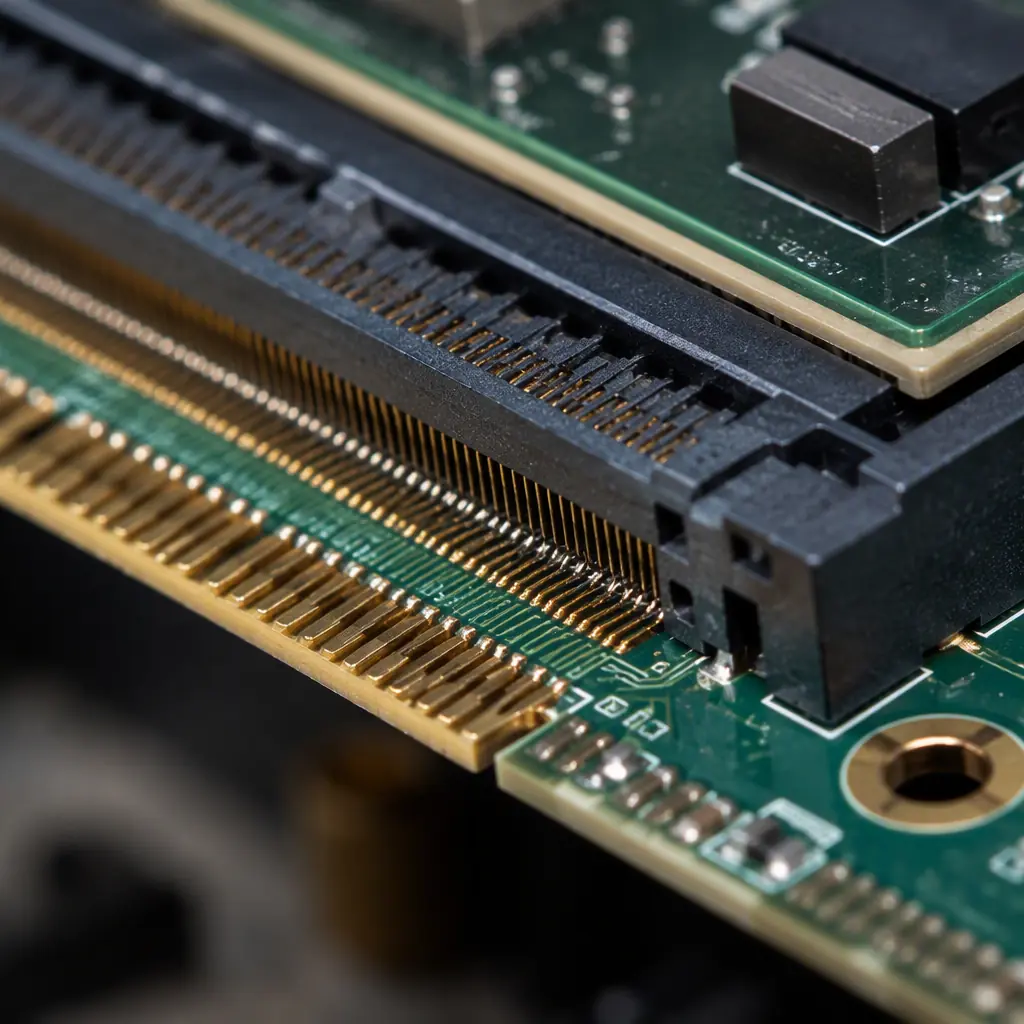
Raspberry Pi Compute Module 4/5 use a 260-pin DDR4 SODIMM edge connector and dominate cost-sensitive products. SMARC and Qseven are standardized industrial form factors (defined by SGET) with long-lifecycle guarantees and wide temperature options — better for medical, transportation, and industrial control where a 10-year supply commitment matters. For very compact designs, board-to-board modules (0.4-0.5 mm pitch mezzanine connectors) save height. The form factor choice sets your connector, mechanical envelope, and available I/O.
Read the Connector's Current and Signal Ratings Before Layout
An SoM connector carries both power and high-speed signals. Check the per-pin current rating for the power pins — a CM4-style connector has specific pins rated for the 5 V input, and exceeding them melts connectors. Check the high-speed pin assignments: which pins are the PCIe lanes, USB pairs, and display lanes, and whether they have dedicated ground pins between them. The datasheet's recommended footprint and breakout pattern are the starting point for your layer count. Our high-speed connector guide covers breakout routing in depth.
Plan the Mechanical Stack From Day One
The module sits on top of the carrier, so the stack height (module + connector + carrier) must fit your enclosure. A SODIMM connector adds ~6-8 mm; mezzanine connectors 2-5 mm. Plan standoffs, heat-sink clearance above the module, and access to the module's antenna connectors or microSD. Late mechanical changes are the most expensive kind — lock the stack height before layout starts.
Power Tree Design: From Input to 0.8 V Core
The carrier board's first job is feeding the module clean, sequenced power. Most modules take a single main input (5 V or 12 V) and regulate internally, but the carrier still needs its own rails for peripherals, and the input path must handle the module's peak current.
Size the Input Path for Peak, Not Average, Current
A quad-core module can draw 1.5-3 A at 5 V under load, with transients during boot and Wi-Fi transmission. Size the input connector, fuse, and trace copper for the peak with margin — a 2 oz copper pour for the main input is common, and the input bulk capacitance (220-470 µF) goes right at the connector. Voltage drop in a thin input trace at 3 A causes brownouts that are infuriating to debug. Our current capacity guide gives the copper math.
Design the Peripheral Rails as a Clean Tree
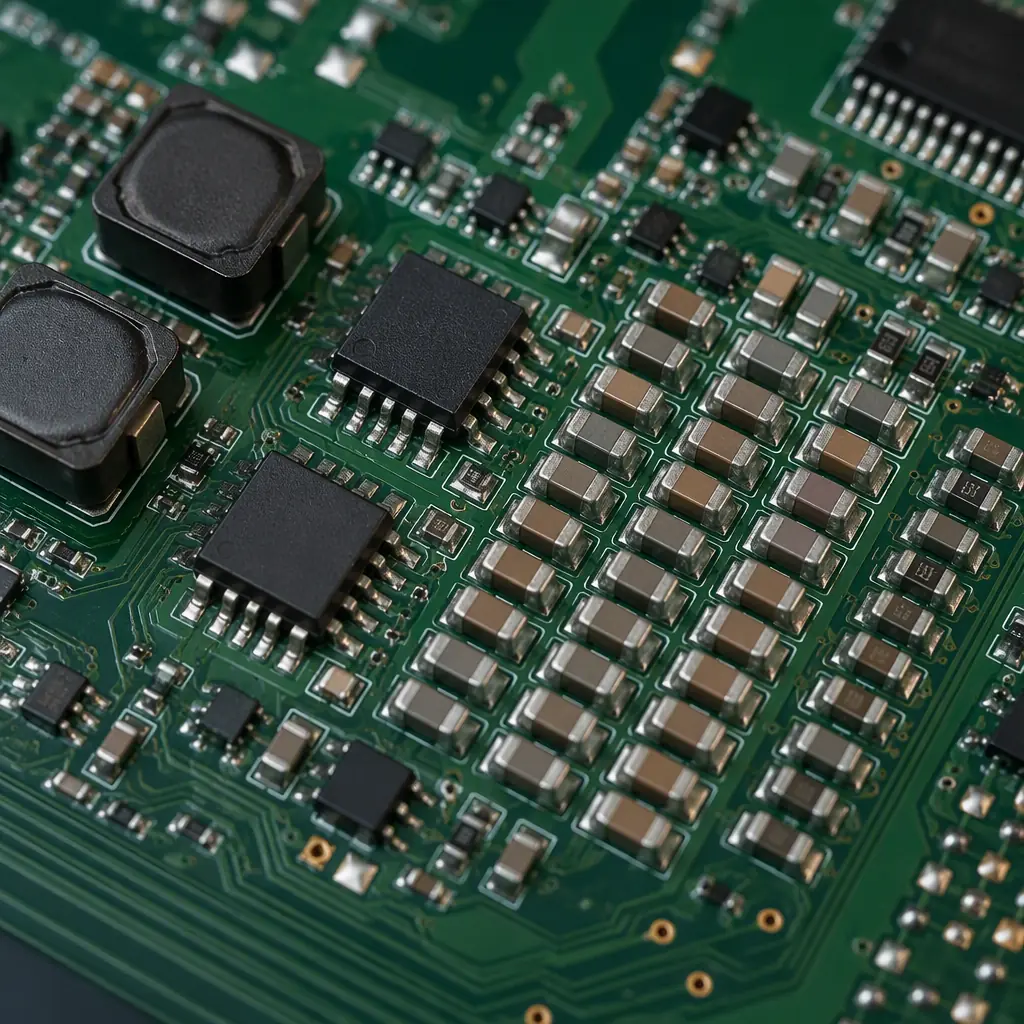
Peripheral rails (5 V for displays, 3.3 V for sensors, 1.8 V for level shifters) come from small buck converters or LDOs on the carrier. Give each rail its own local decoupling at the load, keep the switchers' switching nodes short, and sequence the rails if any peripheral requires power-on order. A power tree diagram in the schematic — input, converters, loads, with current estimates per branch — is the document your DFM reviewer will thank you for. Our power integrity guide covers decoupling and plane design.
Watch the PDN Impedance at the Module Connector
The module's internal regulators need a low-impedance input supply. That means solid power planes under the connector, decoupling right at the power pins (both bulk and 100 nF RF-class caps), and no routing of high-current paths through vias sized for signals. A 0.5 A rail through a single 0.3 mm via is a 30-50 mV drop you did not plan for — parallel vias for every power connection.
High-Speed Routing on the Carrier
The carrier's signal-integrity work concentrates on the interfaces between the module connector and your product's I/O: PCIe, USB 3.x, MIPI CSI/DSI, HDMI, and Ethernet. Our signal integrity guide covers the general method; here are the carrier-specific rules.
Respect the Module Vendor's Routing Guidance
Module vendors publish routing recommendations for each interface — recommended impedance (85 Ω for PCIe and MIPI, 90 Ω for USB 3.x, 100 Ω for Ethernet), trace length limits, and reference-plane rules. Follow them exactly. The module was validated with those constraints; deviating from them moves the risk onto your board. If the module vendor provides a reference carrier design, start from its stackup and routing strategy.
Control the Breakout From the Connector
The pins of an SoM connector are dense, and the first 5-10 mm of routing out of the connector is where impedance control is hardest. Use the connector's recommended breakout, keep pairs adjacent and length-matched from the pin out, and avoid vias in the immediate breakout zone if the layer count allows. If vias are unavoidable (they often are), pair them with ground vias. Our backdrilling guide covers via stub control when the stackup is thick.
Keep Diff Pairs on One Layer and One Reference Plane
Route each differential pair entirely on one signal layer with a continuous reference plane underneath — no crossing plane splits, no reference-plane changes without stitching vias. Length-match within the pair (usually ±0.1-0.5 mm depending on the interface) and between lanes of a bus where the spec requires it. On a 4-6 layer carrier, put the high-speed pairs on the outer layers or on a dedicated signal layer adjacent to ground; our layer count guide helps you pick the stackup.
Add ESD Protection at the External Connectors
USB, HDMI, and Ethernet ports are the entry points for electrostatic discharge. Put ESD protection (TVS diodes) directly at each external connector, before any series elements, with short, low-inductance paths to chassis or signal ground. This is a carrier board afterthought that causes endless field failures if skipped — and it is invisible to functional testing until units die in the field. Our ESD control guide covers the program-level requirements.
Antenna and RF for Wireless SoMs
Modules with Wi-Fi, BLE, or cellular bring their own RF section, but the antenna is usually on the carrier — which means the antenna design problem is still yours.
Use U.FL/IPEX Connectors and External Antennas for Industrial Products
For products where range matters, route from the module's RF pin to a U.FL connector on the carrier edge and use an external antenna. The RF trace between the module and the connector must be a controlled 50 Ω line with the module's recommended clearance — a short, well-grounded run. For cost-sensitive consumer designs, a PCB trace antenna on the carrier can work, but the antenna then competes with the module's own radiation and the enclosure. See our PCB antenna design guide for the design rules.
Keep Antenna Keep-Outs Clear on Every Layer
If the carrier hosts a trace or chip antenna, enforce the keep-out on all layers — no copper pour, traces, or components in the antenna zone, including on inner layers. A ground pour under a chip antenna's clearance area detunes it completely. Add this to the DFM review checklist; it is a top cause of wireless products with half their designed range.
Thermal and Mechanical: Heatsinks, Enclosures, and Warpage
Modules run hot — a quad-core SoC can dissipate 5-15 W — and the carrier board is the thermal path to the enclosure.
Design the Thermal Path, Not Just the PCB
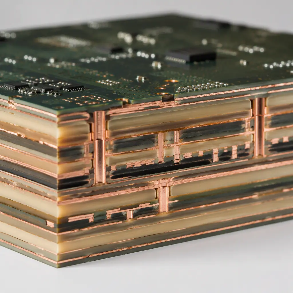
Most modules have a top heat-spreader or expose the processor for a heatsink. The carrier board contributes via thermal vias under the module's power section and, for high-power modules, a metal core or heavy copper layer in that zone. Specify thermal vias (filled or tented, 0.3-0.5 mm, arrayed under the hot area) in the fabrication drawing. Our thermal management guide covers the via and copper strategies.
Control Warpage for Connector Reliability
A carrier board that bows under the module connector causes intermittent contact failures that are nearly impossible to diagnose in the field. Keep copper balance reasonably even across the board, avoid large solid pours on one side only, and consider a 1.6-2.0 mm board thickness for modules with tall connectors. Warpage control matters more on carrier boards than on most designs because of the long connector line. Our warpage guide covers the specifics.
Plan the Assembly Sequence With Your CM
Carrier boards are often double-sided with the SoM connector on one side and peripherals on the other. Confirm the assembly sequence with your manufacturer: which side is populated first, whether the connector is press-fit or SMT, and whether the module is assembled at your site or the factory's. Box-build — carrier, module, enclosure, and final test — is where turnkey manufacturing saves real time. Our turnkey assembly guide explains the scope.

DFM for Carrier Boards: What the Fab Needs From You
Carrier boards concentrate the DFM risk in a few places: the connector footprint, the impedance-controlled pairs, and the mixed assembly. Specify these on the drawing:
Impedance Coupons With Per-Panel Reporting
Request coupons for every impedance class on the board (85/90/100 Ω), measured per panel and reported. The coupon stackup must match the real board. This is the single most common gap between a design that simulates well and a board that measures well. Our impedance control guide covers the coupon requirements in detail.
Connector Assembly and Inspection Requirements
Specify the connector attach method (press-fit vs SMT), the solder paste and stencil requirements for fine-pitch connectors, and the inspection level — X-ray for hidden solder joints under shields and high-pin-count connectors, AOI for the rest. A press-fit SoM connector needs accurate hole size and plating, verified on first articles. Our inspection guide covers the method mix.
Panelization and Test Points
Panelization must keep the connector area flat and clear of V-score stress. Add ICT or flying-probe test points for the critical rails and interfaces on the carrier, and a test strategy that includes a module-bring-up test at the factory if you are using turnkey assembly. Our design for testability guide covers test point placement.
Summary: The Carrier Board Checklist
A carrier board that ships reliably is built on a module form factor matched to the product's lifecycle, a connector treated with respect for its current and signal ratings, a power tree sized for peak currents with clean sequencing, high-speed pairs routed to the module vendor's exact guidance, antennas given their keep-outs, a thermal path designed in from the start, and a fabrication drawing that specifies impedance coupons, connector inspection, and warpage control. Done this way, the SoM approach delivers exactly what it promises: fast time-to-market with low hardware risk.
At Huaxing PCBA we manufacture carrier boards up to 32 layers with impedance control to ±5%, mixed laminates, press-fit and fine-pitch SMT connector assembly, X-ray inspection, and full turnkey box-build with bring-up testing. Our DFM review checks the connector breakout, impedance stackup, power input path, thermal via arrays, and assembly sequence before tooling. Read our server PCB guide for the high-layer-count side of the same discipline, or send your files for a free DFM review and quote.
