
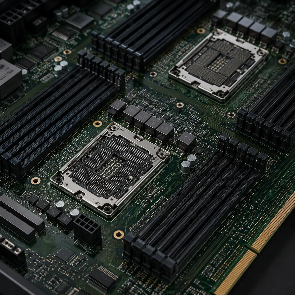
Data center server motherboards are among the most demanding PCB designs in the electronics industry. A single hyperscale server board may carry 400G Ethernet controllers, 32-core processors, DDR5 memory channels, and PCIe 5.0 lanes, all on a 20-32 layer PCB that must maintain signal integrity while dissipating over 100W of thermal load. For procurement engineers sourcing these boards, understanding the manufacturing requirements is not optional. It is the difference between a reliable cloud infrastructure and a rack full of field failures.
At Huaxing PCBA, we manufacture high-layer-count PCBs for server and networking applications at our 15,000 m² facility in Shenzhen. With 8 SMT lines, IATF 16949 certification, and in-house impedance TDR testing, we support everything from prototype backplanes to volume production of compute node boards. This guide covers the material, stackup, and thermal decisions that determine whether a server PCB meets its performance targets.
Layer Count and Stackup Architecture for Server Boards
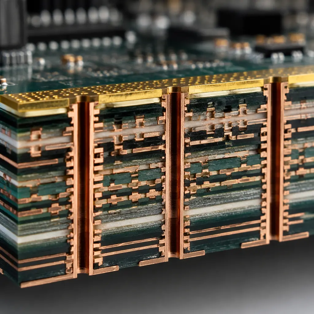
Server PCB layer count is driven by three factors: signal escape from high-pin-count BGAs, power delivery network (PDN) impedance requirements, and isolation between sensitive analog and high-speed digital domains. A modern dual-socket server board typically demands 18-26 layers; a switching backplane for 400G fabric can exceed 32 layers.
BGA Escape Routing Drives Layer Count
A single LGA-4677 server socket has over 4,600 pins. Routing all DDR5, PCIe 5.0, and power pins requires at least 8-10 signal layers with blind and buried vias. Each additional high-pin-count component (network controller, CXL accelerator) adds 2-4 layers. Our facility supports blind, buried, and back-drilled vias up to 32 layers with 0.2mm laser-drilled microvias.
PDN Design Requires Dedicated Power Layers
Server CPUs draw 200-400W at sub-1V core voltages, demanding power plane impedance below 1 mΩ. A proper stackup dedicates 4-6 layers to power distribution with 2oz-4oz copper. See our copper weight selection guide for specifying heavy copper layers in mixed-weight stackups.
Signal Isolation Between Clock, RF, and Digital Domains
Server boards mix 100G PAM4 serial links, DDR5 memory buses at 5600 MT/s, and PCIe 5.0 at 32 GT/s. Crosstalk between adjacent signal layers must be below -40 dB. Our PCB stackup design guide covers the shielding and ground-plane strategies that make mixed-signal server boards manufacturable.
Procurement Reality: Most Chinese PCB fabs quote 20+ layer server boards at 8-12 week lead times. Huaxing delivers production-qualified 24-layer server boards in 5-7 working days using domestic supply chains for Isola and Panasonic-equivalent laminates, without the export-control delays that affect Rogers and other ITAR materials.
Low-Loss Laminate Selection for 56 Gbps and Beyond
Signal loss at 28 GHz Nyquist frequency (56 Gbps PAM4) eliminates standard FR-4 from consideration. The material choice cascades through every downstream decision: dielectric thickness, trace width, via stub length, and cost. Three material tiers dominate the server PCB market in 2026.
| Material | Dk @ 10GHz | Df @ 10GHz | Max Data Rate | Relative Cost |
|---|---|---|---|---|
| FR-4 (standard) | 4.2-4.5 | 0.020 | ≤ 10 Gbps | 1.0× |
| Mid-Loss (Megtron 4 / IT-170GRA) | 3.6-3.8 | 0.008-0.010 | ≤ 28 Gbps | 2.5× |
| Low-Loss (Megtron 6 / IT-968G) | 3.4-3.6 | 0.004-0.006 | ≤ 56 Gbps | 4.0× |
| Ultra-Low-Loss (Megtron 8 / IT-988G) | 3.2-3.4 | 0.002-0.003 | 112 Gbps+ | 7.0× |
For most cloud server boards operating at PCIe 5.0 (32 GT/s) or 100G Ethernet (53.125 Gbps per lane), low-loss materials like Megtron 6 or IT-968G provide the right balance of signal integrity and cost. Ultra-low-loss materials are reserved for 400G/800G switch backplanes where every fraction of a dB matters.
Verify Glass-Style and Resin Content with Your Fab
Low-loss laminate performance varies by glass weave style. 106 and 1035 glass styles minimize skew at high frequencies but cost more. Open-weave 1080 glass in low-loss resin can create impedance discontinuities above 25 GHz. Our engineering team reviews your stackup before quoting to flag glass-style issues that cause field failures. See our laminate selection guide for the full comparison.
Specify Back-Drilling for Via Stubs Above 5 Gbps
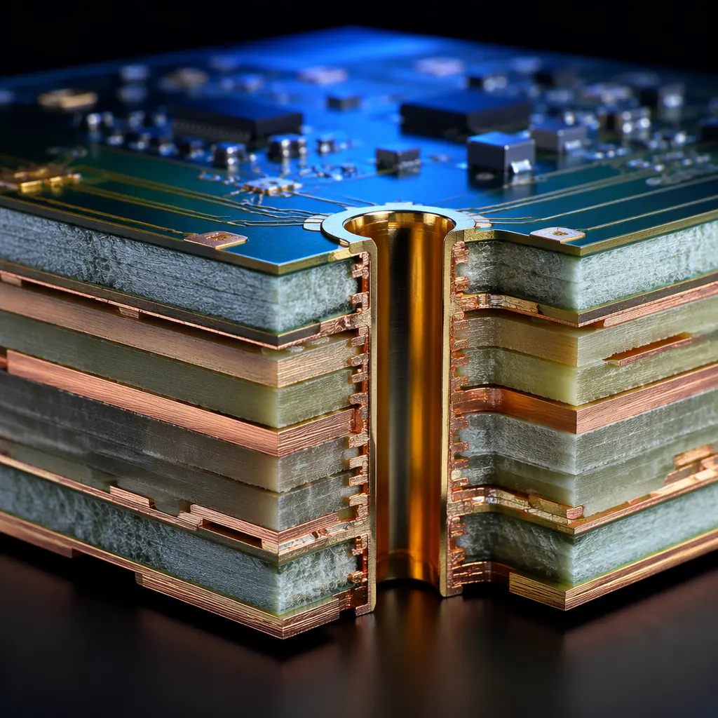
An un-removed via stub creates a quarter-wave resonator that causes severe insertion loss at specific frequencies. For 56 Gbps PAM4 signals, stubs must be removed to within 6 mils of the signal layer. Our back-drilling guide covers stub length tolerances and inspection methods.
Thermal Management for 100W+ Server Processors
A single server CPU socket may dissipate 200-400W. Multiply by two sockets, add four DIMM channels, network controllers, and voltage regulators. And the total board-level thermal load exceeds 800W. The PCB itself must carry heat away from hot spots without delamination or warpage.
Heavy Copper Inner Layers as Thermal Spreaders
Embedding 3oz-6oz copper planes in the inner layers directly below CPU and VRM zones acts as a lateral heat spreader, reducing hot-spot temperatures by 8-15°C compared to 1oz planes. Our heavy copper PCB guide shows the manufacturing considerations for mixed-weight stackups.
Thermal Via Arrays Under BGA Packages
Dense thermal via arrays (0.3mm pitch, 0.15mm hole) under CPU BGAs provide the lowest thermal resistance path to internal copper planes. Via-in-pad with conductive fill adds ~15% to board cost but improves thermal conductivity by 300% over standard plated vias. Review our via fill types comparison for trade-offs.
High-Tg Material for Lead-Free Assembly and Long-Term Reliability
Server boards undergo multiple reflow cycles during assembly (SMT top, SMT bottom, selective soldering). High-Tg FR-4 (Tg ≥ 170°C) or polyimide-based laminates prevent delamination during repeated thermal cycling. All Huaxing server-grade laminates are rated Tg 170-180°C minimum. See our materials comparison guide for Tg vs. Td specifications.
Key Takeaway: Thermal management is a PCB design problem, not just a heatsink problem. The difference between a server board that throttles at 85°C ambient and one that runs reliably at 95°C is often the copper weight and via structure specified in the fabrication drawing, not the heatsink selection.
IPC Class and Reliability Requirements for Server PCBs
Data center hardware operates 24/7/365 with a target service life of 5-7 years. Unlike consumer electronics, server boards cannot be field-repaired, a single PCB failure triggers a rack-level service event. The manufacturing quality standard matters.
| Requirement | IPC Class 2 | IPC Class 3 (Recommended) |
|---|---|---|
| Annular ring minimum | 0.05mm breakout allowed | 0.025mm, no breakout |
| Plating void allowance | ≤ 5% of hole wall | No voids permitted |
| Solder joint inspection | Visual sampling | 100% AOI + X-Ray on BGA |
| Conformal coating | Optional | Required for humidity > 60% |
| Impedance tolerance | ±10% | ±5% with TDR report |
Most hyperscalers specify IPC Class 3 for server motherboards and backplanes. The incremental cost (typically 15-25% over Class 2) is justified by the cost of a single rack-level failure: a $500 board failure in a $250,000 server chassis costs far more in downtime and field service. Our IPC Class 2 vs Class 3 guide provides a detailed cost-benefit analysis.
Summary: Specifying Server PCBs for Manufacturability
Data center server PCB procurement reduces to four decisions: layer count (determined by BGA pin count and PDN requirements), laminate grade (low-loss for 56 Gbps, ultra-low-loss for 112 Gbps), copper weight (3oz-6oz inner layers for thermal), and IPC class (Class 3 for hyperscale, Class 2 for cost-sensitive edge servers).
At Huaxing PCBA, we manufacture up to 32-layer server PCBs with ±5% impedance control, back-drilling to 6 mil stub length, and full AOI + X-Ray inspection. Our 8 SMT lines support prototype runs of 5-50 units and volume production of 5,000+ units per month with 24-hour quick-turn engineering samples. Read our supplier audit checklist or contact our engineering team to review your server board stackup before quoting.
