
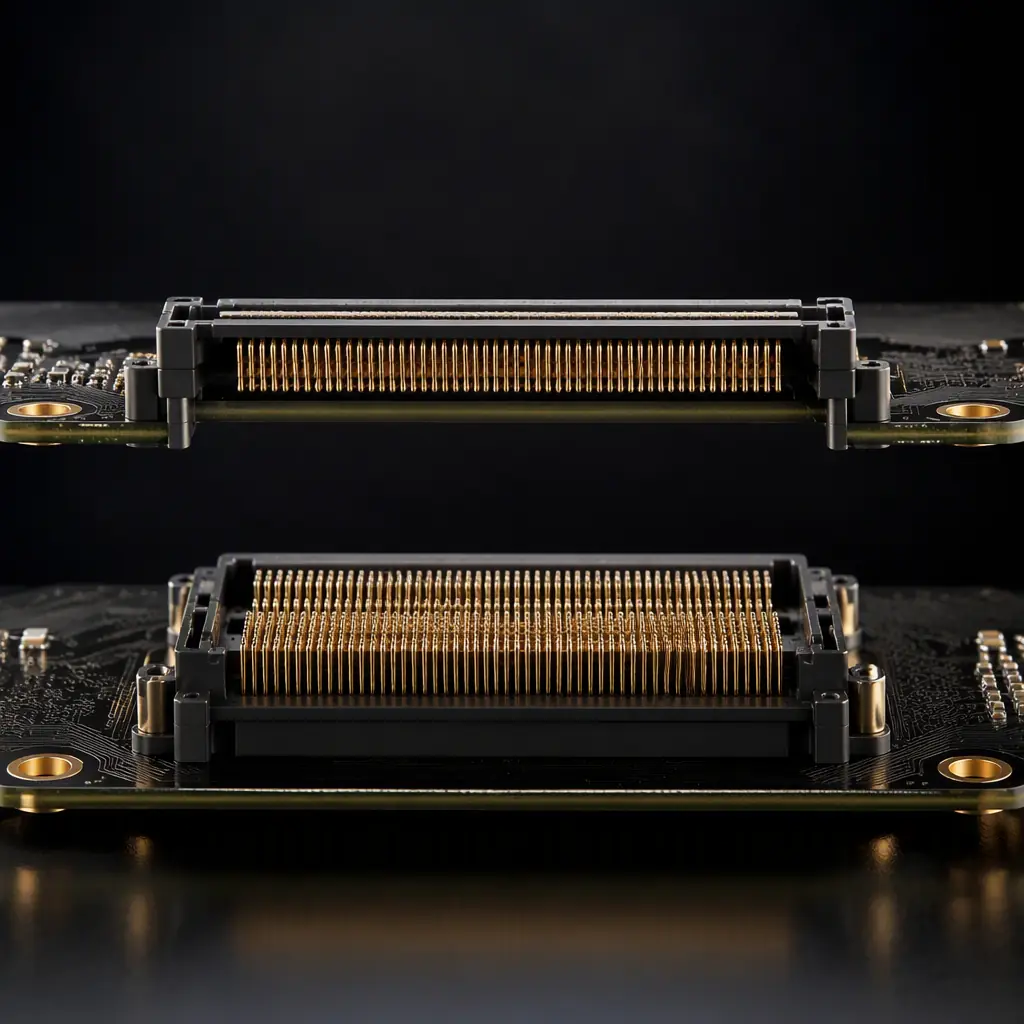
Every high-speed system eventually crosses a connector: a mezzanine board stacked over a motherboard, a line card plugged into a backplane, a module seated on a carrier. At 10 Gbps the connector and its breakout are a manageable problem; at 25, 56, and now 112 Gbps (PAM4), the connector pin field is often the limiting element of the whole channel. The PCB work around a connector — the breakout pattern, the via transitions, the return-path vias — determines whether the link closes with margin or fails intermittently in the field.
Huaxing PCBA manufactures high-layer-count boards for networking, server, and industrial customers — stackups up to 32 layers, backdrilling for via-stub control, tight-impedance differential pairs, and press-fit connector assembly. This guide covers how to choose board-to-board, mezzanine, and backplane connectors, how to route the breakout and manage vias, and what to specify on the fabrication drawing so the channel performs as designed.
Connector Families and When to Use Each
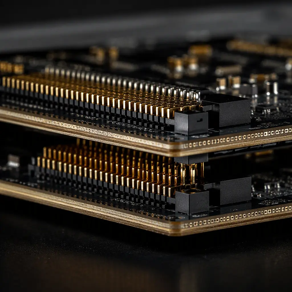
High-speed connectors come in three broad families, and the choice between them is driven by the system architecture — how the boards stack, how often they are serviced, and what data rate the channel must carry.
| Connector Family | Typical Pitch | Data Rate | Best For |
|---|---|---|---|
| Board-to-board (stacking) | 0.4-0.8 mm | up to 10-25 Gbps | Module-on-carrier, sensor boards, compute modules |
| Mezzanine (high-density) | 0.5-1.27 mm | 10-56 Gbps | Processor/FPGA mezzanines, stacked compute |
| Backplane (card edge / orthogonal) | 1.9-2.5 mm column pitch | 25-112 Gbps PAM4 | Line cards, switches, routers, servers |
The data rate is the first constraint: a connector rated for 56 Gbps PAM4 has a fundamentally different internal geometry (twin-ax style contacts, ground shielding between pairs) than a 10 Gbps part. Choosing a connector rated well above your actual link rate is the cheapest insurance — the connector cost difference is small compared with a channel redesign. Our network switch PCB guide covers the system-level architecture these connectors support.
Selecting the Right Connector for Your Link
Connector selection is where most high-speed projects make their first mistake: picking a part for mechanical fit and discovering too late that its electrical rating does not match the link budget. Work through the checklist below before committing to a part number.
Match the Rating to the Worst-Case Link, Not the Nominal One
A connector rated at "25 Gbps" may be specified for NRZ at a specific loss budget and trace length. If your channel runs the connector at the far end of a long backplane trace with multiple vias, the effective margin is much smaller. Compare the connector's insertion loss and return loss specs against your total channel budget — not just the bit rate. The vendor's differential insertion loss at the operating frequency (e.g., 14 GHz for 56 Gbps PAM4) is the number that matters. Our signal integrity guide explains the channel budget method.
Check the Pin-Field Breakout Before the Footprint
Every high-speed connector has a recommended breakout pattern — the exact routing of the differential pairs out of the pin field, published in the datasheet. The breakout pitch (how many rows deep you can route before needing vias) determines how many layers the board needs. A 0.5 mm pitch mezzanine connector with 4 rows of signals typically requires 8-12 layers for a clean breakout; a backplane connector with shielded columns needs a specific via pattern. Verify the breakout fits your stackup before layout starts — this is the single most common cause of late-layer-count increases. Our layer count guide covers the trade-offs.
Plan for Press-Fit or Solder Attachment
High-speed connectors attach by press-fit compliant pins (preferred for backplane and high-pin-count parts — no solder, field-replaceable) or by surface-mount solder. Press-fit needs plated through-holes with a specific finished hole size and a board thickness within the connector's range, plus a press fixture on the assembly line. SMT high-speed connectors need precise solder paste volume and often a vacuum or low-void profile for the larger ground pins. Our press-fit guide covers the hole and plating requirements in detail.
Key Takeaway: Select the connector against your channel budget, verify the breakout fits your planned layer count, and confirm the attachment method matches your assembly line. Connector selection done this way removes 80% of the late-stage signal-integrity surprises on high-speed boards.
Breakout Routing: Getting Out of the Pin Field Alive
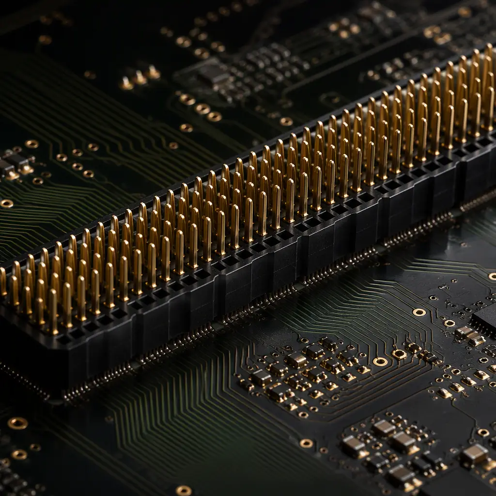
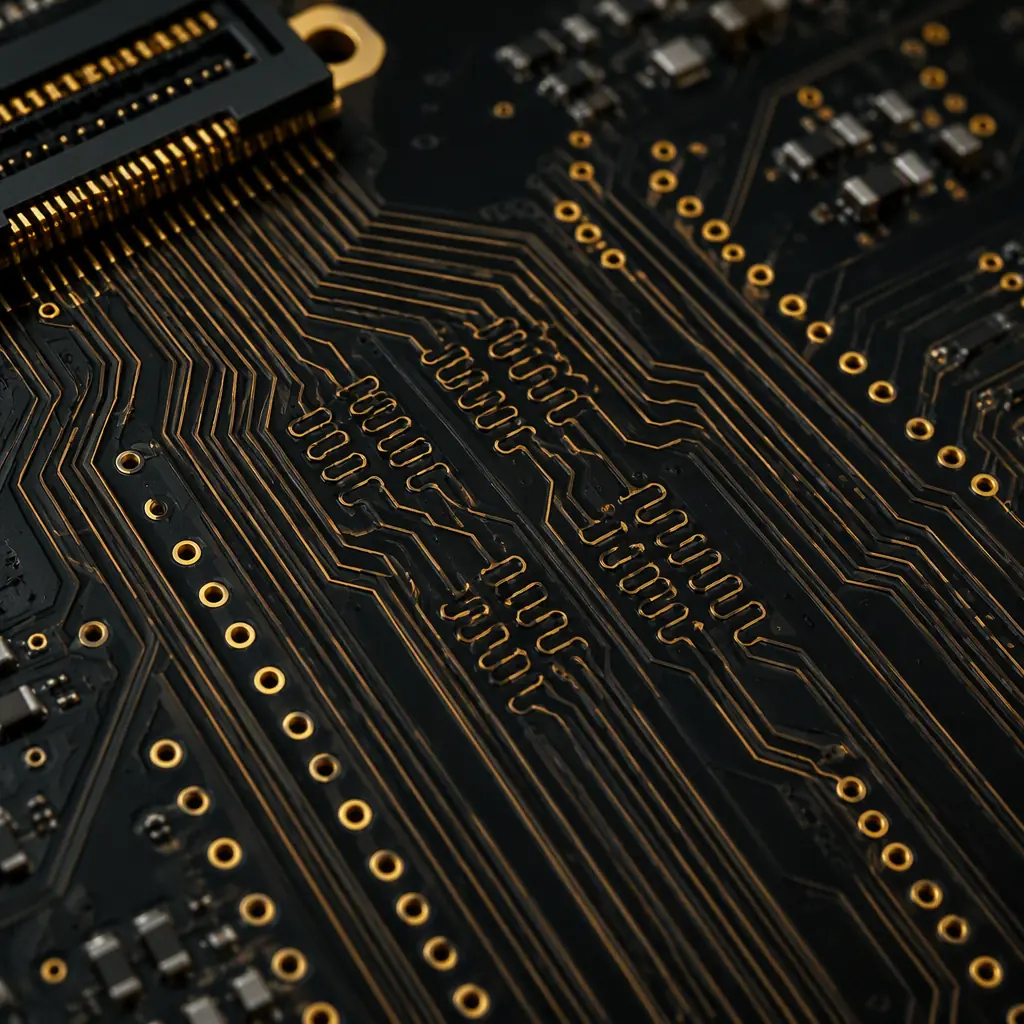
The breakout — routing from the connector pins to the first free routing channel — is where high-speed designs are won or lost. In the pin field, trace widths shrink, spacing tightens, and impedance control becomes difficult. The breakout strategy determines how many layers you need and how much crosstalk the channel starts with.
Follow the Vendor Breakout Pattern Exactly
Connector vendors publish recommended breakout layouts with specific trace widths, spacing, and via placement for each data rate. These patterns are simulation-verified — deviating from them (thinner traces to fit more channels, tighter spacing to save layers) shifts the impedance and adds crosstalk. The breakout is not a place for improvisation. If the vendor pattern does not fit your stackup, change the stackup or the connector, not the pattern. Our stackup design guide explains how to size planes and dielectrics for breakout impedance.
Manage the Via Transition: Backdrill, Ground Vias, and Stub Control
Every signal via in a high-speed channel has a stub — the unused portion of the plated barrel — that resonates and notches the channel at specific frequencies. Above 10 Gbps, backdrilling (drilling out the unused stub) is standard; above 25 Gbps it is mandatory. Place ground vias around signal vias to control the return path, and keep the signal-via antipads sized per the vendor recommendation. Our backdrilling guide covers stub effects and drill depth control in depth.
Keep Pair Spacing and Ground Shielding Consistent
In the breakout, differential pairs must keep their nominal spacing (the gap between the + and - traces) and pair-to-pair separation per the impedance target. When pairs run parallel for more than a few millimeters, add ground stitching between them to control crosstalk. The impedance in the breakout zone should match the rest of the trace — a 100 Ω target everywhere, including under the connector footprint. Our crosstalk guide covers spacing and shielding rules.
Stackup and Material Choices for Connector Channels
The board material and stackup determine whether the connector's rated performance is actually achievable. A 56 Gbps connector on a lossy FR-4 board with poor plane spacing will not deliver 56 Gbps — the board becomes the bottleneck.
Match the Laminate to the Data Rate
Standard FR-4 (Dk ~4.2, Df ~0.020) is fine up to about 10 Gbps with short traces. Above 25 Gbps, low-loss laminates (Df below 0.010, such as Megtron 6/7 or Isola equivalents) are required, and at 112 Gbps the material choice dominates the channel loss budget. The connector vendor's performance curves assume a specific material class — using a cheaper laminate voids the connector's rated performance. Our laminate selection guide compares the material families.
Control Plane Spacing for Impedance and Crosstalk
The dielectric thickness between signal layers and their reference planes sets both the trace impedance and the crosstalk coupling. Tight plane spacing (thin dielectric) reduces crosstalk but forces thinner traces for the same impedance; the stackup must balance trace width, spacing, and plane distance. Specify the impedance targets and the stackup on the fabrication drawing, and verify with coupons. Our tolerances guide covers what the fab actually holds.
Plan the Reference-Plane Transitions
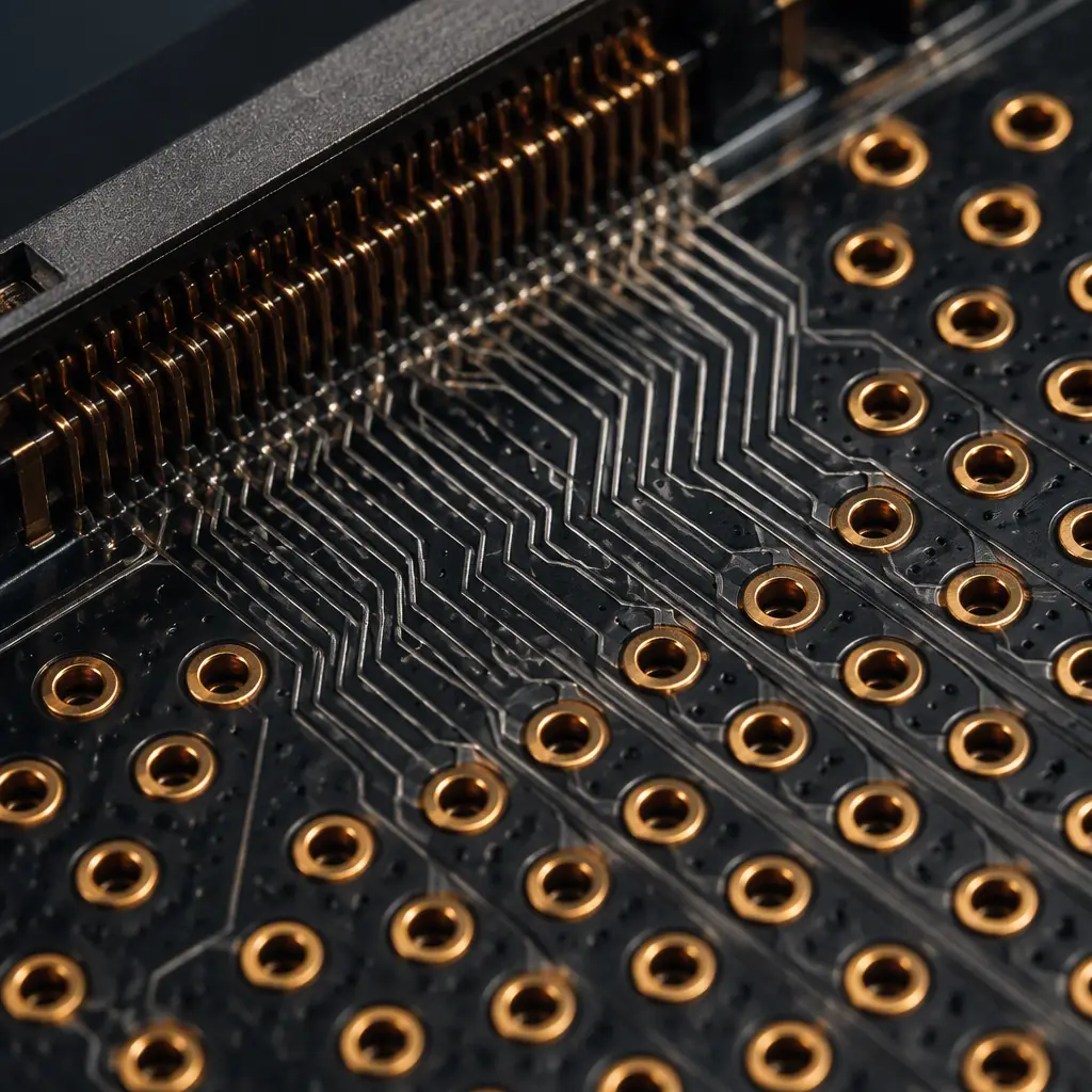
When a differential pair changes reference planes (from one ground layer to another) near a connector, the return current must have a path — place ground vias at the transition. Floating copper or a split plane under a connector pin field creates a return-path discontinuity that shows up as a resonance notch. Every reference-plane change in the breakout zone needs its own ground-via stitch. Our via technology guide covers the via patterns for clean transitions.
Verification: Simulation, TDR, and Eye Diagrams
A high-speed connector channel cannot be verified with a multimeter. The design must be checked with simulation before tooling and with measurements on the first articles. This is not optional above 10 Gbps — it is the difference between a board that works and a board that "mostly works".
Simulate the Full Channel Before Tooling
Model the complete channel — driver, trace, vias, connector, trace, receiver — using the connector vendor's S-parameter models and your stackup. Check insertion loss, return loss, and crosstalk against the link budget with margin (typically 3 dB or more). If the channel closes in simulation with less than 2-3 dB margin, the physical board will fail in production. This simulation is standard practice for networking and server boards; your manufacturer should support reviewing the results. Our server PCB guide covers the verification flow for high-layer-count boards.
Measure TDR and Eye Diagrams on First Articles
On the first articles, measure the channel with a Time Domain Reflectometer (TDR) to verify impedance through the connector and breakout, and capture eye diagrams at the operating rate. A TDR sweep of the connector zone shows exactly where the impedance deviates — typically at the via and the connector pin. Eye diagrams show the real margin at the receiver. Compare the measurement against simulation; a >5% deviation means something in the stackup or breakout differs from the model. Our testing methods guide places these measurements in the full test strategy.
Verify Backdrill Depth and Via Quality in Production
Backdrill depth is a production-controlled parameter: too shallow leaves a stub, too deep breaks the connection to the plane. Specify the backdrill depth tolerance on the drawing and verify with cross-sections on first articles and lot samples. Similarly, via wall quality (no voids, complete plating) is verified by microsection. Our microsection guide covers how to read these verification reports.
Manufacturing Requirements for Connector-Heavy Boards
High-speed connector boards stress the manufacturing process in specific ways: the impedance control must hold across the panel, the press-fit holes must be drilled and plated to tight tolerance, and the assembly must handle heavy connectors without skewing.
Impedance Coupons on Every Panel, Reported Per Panel
For every panel of a high-speed board, the fab should produce impedance coupons measured and reported against the ±10% (or tighter) target. Do not accept "verified" without the data. The coupon must represent the actual stackup — same dielectric thickness, same trace geometry — not a simplified test structure. Our quality metrics guide covers what to track across lots.
Hole Quality for Press-Fit Pins
Press-fit connectors demand finished hole diameters within ±0.05 mm of spec, smooth plating, and no burrs — a burr or undersized hole scrapes the compliant pin and breaks the connection. Specify the hole tolerance, and verify with a press-fit insertion test on first articles. Copper thickness in the hole must meet the current requirement for power pins (often 25-50 µm). Our current capacity guide covers plating thickness for power paths.
Assembly: Support, Alignment, and Inspection
Heavy backplane connectors need board support during assembly to prevent warpage, and the placement must hold tight coplanarity for SMT parts. After assembly, X-ray inspection verifies solder joints on SMT high-speed connectors, and a seating-height check verifies press-fit insertion. Specify "100% visual + X-ray on first article, lot-sample X-ray" for the connector joints. Our inspection guide covers the method mix.
Summary: The High-Speed Connector Checklist
A high-speed connector channel that closes with margin is selected against the channel budget, laid out with the vendor breakout pattern, disciplined through the via transitions with backdrilling and ground stitching, built on a laminate that matches the data rate, verified by simulation and TDR/eye measurements, and manufactured with per-panel impedance reporting and tight press-fit hole control.
At Huaxing PCBA we manufacture high-speed connector boards up to 32 layers with low-loss laminates, backdrilling to ±0.05 mm depth control, per-panel impedance coupons, press-fit assembly with insertion testing, and X-ray inspection of connector joints. Our DFM review checks the breakout pattern, via and backdrill plan, stackup impedance targets, and hole tolerances before tooling. Read our network switch PCB guide to prepare your design, or send your files for a free DFM review and quote.
