
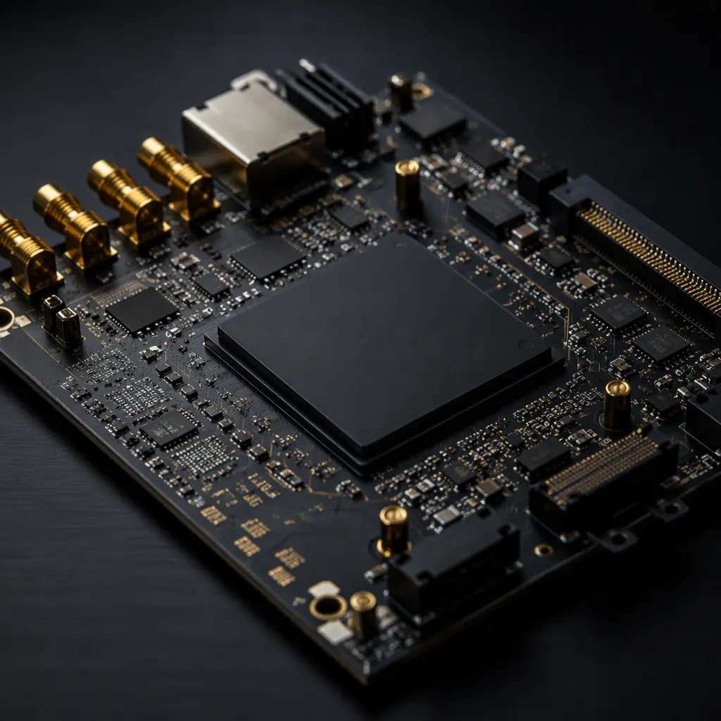
FPGAs are the workhorses of industrial control, defense electronics, AI edge inference, and test instrumentation — and they are among the most demanding devices to put on a PCB. A mid-range FPGA draws current from four or more power rails, routes hundreds of high-speed I/O pins, and comes in a BGA package whose assembly tolerances are measured in micrometers. Most FPGA layout failures are not logic errors; they are power delivery, stackup, or assembly problems that show up weeks after the first boards arrive.
Huaxing PCBA manufactures FPGA boards up to 32 layers with laser-drilled microvias, ±5% impedance control, and BGA placement down to 0.3 mm pitch across 8 SMT lines. This guide walks through the design decisions that determine whether your board works the first time — power sequencing, the decoupling network, layer count, high-speed routing, and the manufacturing checks that catch problems before production. If you are new to board stackups, our stackup design guide covers the fundamentals first.
Why FPGA Boards Fail Differently
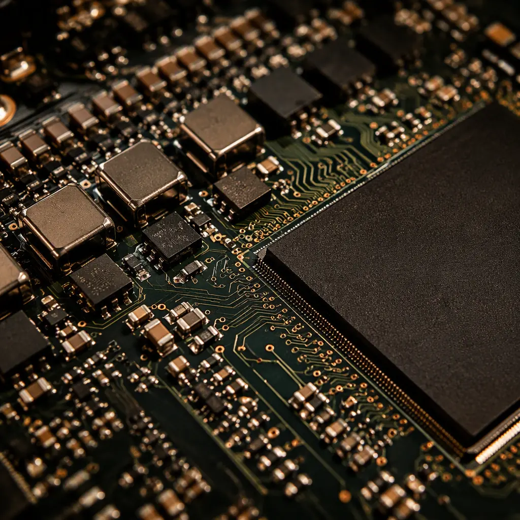
An FPGA is not a microprocessor with a few power pins. A Xilinx or Intel device exposes separate rails for the core logic, block RAM, auxiliary circuits, I/O banks, and high-speed transceivers — each with its own voltage, current draw, and sequencing requirement. On top of that, the package is a large BGA with hundreds of power balls in the center, which means power must be delivered vertically through the board, not along its surface.
The practical consequences: the power system is designed before routing, the stackup must provide clean reference planes for both signals and current return, and the board house must hold tight tolerances on impedance, via drills, and BGA pad geometry. Skipping any of these turns a working schematic into a non-booting board.
Key Takeaway: FPGA layout is power-first. Decide the rail architecture, sequencing, and decoupling budget before placing a single route — the signal layers are the easy part compared to delivering 20 A at 0.85 V with less than 30 mV of droop.
FPGA Power Rails and Sequencing: The Order Matters
Every major FPGA family defines a power-on sequence. For AMD/Xilinx devices, the core rail (VCCINT) must ramp first, followed by VCCBRAM, then VCCAUX, and finally the I/O banks (VCCO). Intel/Altera specifies a similar hierarchy: core before I/O, with the transceiver rails (VCCH, VCCL) sequenced relative to the core. The reason is internal ESD structures — if an I/O rail powers up while the core is still off, current can leak through protection diodes and latch the device.
A typical FPGA rail plan looks like this:
| Rail | Typical Voltage | Typical Current | Sequence Position | Notes |
|---|---|---|---|---|
| VCCINT (core) | 0.72–0.95 V | 5–30 A | 1st | Lowest voltage, highest current — tightest tolerance |
| VCCBRAM | 0.72–0.95 V | 1–4 A | 1st–2nd | Often tied to VCCINT with a filter |
| VCCAUX | 1.8 V | 0.5–2 A | 2nd–3rd | Feeds configuration and analog circuits |
| VCCO (I/O banks) | 1.2 / 1.5 / 1.8 / 2.5 / 3.3 V | 0.5–4 A per bank | Last | Bank voltage depends on interface standard |
| MGTAVCC / MGTAVTT | 1.0 / 1.2 V | 1–3 A | After core | Transceiver analog rails — cleanest supply on the board |
Design the sequencing with dedicated supervisor ICs or a PMIC with programmable sequencing rather than relying on RC delays — RC timing drifts with temperature and tolerances. A power monitor with a reset output that holds the FPGA in configuration until all rails are valid is the cheapest insurance against intermittent boot failures. Our power integrity and PDN design guide covers target impedance and plane design in detail.
The Decoupling Network: 100 nF Is a Starting Point, Not a Plan
FPGA data sheets specify a minimum decoupling capacitance — typically 0.1 µF per power pin pair — but that number assumes ideal placement. What actually matters is the impedance of the whole power delivery network (PDN) from the regulator through the planes to the die. For a core rail at 0.85 V with a 20 A transient, a 5% droop budget leaves only 42 mV, and the PDN impedance must stay below roughly 2 mΩ across the switching frequency range.
Use a Mix of Capacitor Values, Not a Wall of Identical Caps
Parallel resonance between identical capacitors creates impedance peaks. A proven recipe is one 0.1 µF cap per power pin pair plus a distribution of 0.01 µF, 1 µF, and 4.7–22 µF bulk caps near the package. Use X7R or better dielectrics — X5R loses over half its capacitance at DC bias on a 0.85 V rail is marginal, and on 3.3 V rails X5R can drop 60%.
Place High-Frequency Caps on the Bottom Side Directly Under the BGA
For 0.8 mm pitch BGAs, the 0.1 µF caps go on the opposite side of the board, each connected to its power ball via a microvia. The via inductance between ball and cap dominates at high frequency, so keep the loop short — a 0.3 mm via pair has roughly 0.5 nH, which matters at 100 MHz and above. Our via technology guide covers via-in-pad and microvia options.
Budget Bulk Capacitance for the Regulator Loop
The regulator's output capacitors (47–470 µF across the board) handle the low-frequency transient. Spread them around the board edge near the power entry point, not only at the regulator — the plane itself is part of the loop. Confirm the total with a PDN simulation; most EDA tools now include it.

Layer Count and Stackup: How Many Layers Does Your FPGA Board Need?
There is no universal answer, but a practical rule: the number of routing layers equals the number of distinct signal groups plus two reference planes, rounded up. A small FPGA with 100 I/O pins and no transceivers fits on 4–6 layers. A mid-density device with DDR4 and a few gigabit links needs 8–10. A high-end FPGA with dozens of 10–28 Gbps transceivers, multiple DDR banks, and wide parallel buses routinely needs 14–20+ layers.
| Design Class | Typical Layers | Key Stackup Elements | Example Device |
|---|---|---|---|
| Low-density, no transceivers | 4–6 | 2 signal + 2 plane | Cyclone 10, Artix-7 small |
| Mid-density with DDR3/DDR4 | 8–10 | 4–6 signal + 4 plane | Artix-7, Kintex-7 small |
| High-end with 10G+ transceivers | 14–20 | Dedicated transceiver layers, multiple ground planes | Kintex UltraScale, Agilex |
| Large array + many high-speed buses | 20–32 | Blind/buried vias, HDI microvia build-ups | Virtex UltraScale+, Stratix 10 |
Whatever the layer count, three rules hold. First, every signal layer must sit next to a continuous reference plane — never two signal layers back-to-back. Second, the transceiver pairs need their own clean layer or a dedicated zone with no crossing vias. Third, specify impedance control at 50 Ω single-ended and 100 Ω differential with a ±5% tolerance, and require test coupons. Our impedance control guide explains how coupons are measured and what the report should show.
Routing High-Speed I/O: Transceivers, DDR, and LVDS
The routing rules for FPGA I/O depend on the interface. Differential transceiver pairs (10–28 Gbps) need length-matched, impedance-controlled traces with minimal via transitions — each via adds ~0.5 dB of loss and a reflection point. DDR buses need matched lengths within the byte group and a solid reference plane under the whole bus. LVDS and other parallel interfaces need matched skew and controlled spacing to prevent crosstalk.
Route Transceiver Pairs on the Top Layer, Keep Vias Out of the Pair
When a via transition is unavoidable, add a ground stitching via beside each signal via to provide a return path, and keep the pair together through the transition. Avoid routing transceivers over split planes — the return current has nowhere to go and the pair radiates. Our signal integrity guide covers pair routing and via discipline in depth.
Match DDR Lengths Within the Group, Not Just the Bus
DDR4 at 2400 MT/s tolerates roughly ±10 ps of skew within a byte lane. At typical FR-4 propagation (~150 ps/inch), that is about ±1.5 mm of length matching — doable, but only if the reference plane is continuous under the entire bus. Our DDR4/DDR5 design guide has the full routing recipe.
Guard Sensitive Analog Pins from Switching Noise
Transceiver analog rails (MGTAVCC) and any ADC/DAC sections want their own quiet zones with separate filtering. Route digital switching traces at least 3× the trace width away from analog traces, and avoid crossing splits in the analog reference plane.
Configuration, JTAG, and Debug: Design the Test Access In
An FPGA board without a debug strategy is a board that gets reworked. Every design should expose a JTAG header (or pads) for boundary-scan testing and configuration programming, plus a selection of test points on the critical rails.
Route JTAG Pins to a Dedicated Header or Pads
TDI, TDO, TCK, TMS plus target power and ground — the header must be reachable during assembly, so place it on the board edge. If space is tight, a 5-pin pad array works for production programming before final assembly. Boundary scan through JTAG also lets a test engineer verify BGA solder joints without physical probing.
Add Test Points on Every Power Rail
Bring VCCINT, VCCAUX, VCCO, and the transceiver rails out to 0.9 mm test points. During first-article bring-up, these are the fastest way to verify sequencing and droop with an oscilloscope. Our design-for-testability guide lists the test point rules your assembly partner expects.
Choose the Configuration Mode Early
Master SPI (boot from flash), slave selectMAP, or JTAG — the mode pins and the flash device footprint must be on the board from the first layout pass. Adding a boot flash late forces a board revision.
BGA Assembly and DFM: What the Factory Needs From You
Large FPGA packages concentrate every assembly risk: fine pitch, high ball count, and significant warpage when the die and substrate heat up. The design decisions that keep assembly yields high:
Use Via-in-Pad for 0.8 mm Pitch and Below
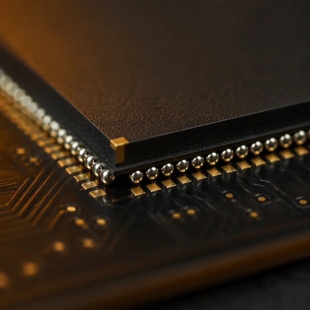
At 0.8 mm pitch there is no room for dog-bone fanout — the via must go directly in the pad, filled and plated. Specify VIPPO (via-in-pad plated over) so solder paste does not wick into the via. Our BGA assembly guide covers fanout and paste stencil rules.
Plan the Stencil and Reflow Profile for the Biggest Package
The stencil aperture for 0.8 mm pitch BGA is typically 0.35–0.40 mm with a 1:1 area ratio. The reflow profile must satisfy the FPGA's peak temperature limit (usually 245 °C max at the package surface for lead-free) while still reaching full wetting on large ground planes. Our reflow profile guide covers the trade-offs.
Require X-Ray Inspection of Every FPGA BGA
Visual inspection cannot see solder balls under the package. X-ray must check for shorts, opens, and voids in the critical power balls — voids above 25% of ball area on a core power ball can cause hot spots. Our AOI/X-ray/SPI inspection guide explains what the X-ray report should contain.
Watch Warpage on Large Packages
A 35×35 mm BGA with a large die can warp during reflow, lifting corner balls. Mitigations: keep the board copper balanced, use a profile with adequate soak, and confirm the board meets the flatness spec (typically ≤0.75% bow per IPC-6012). If the package is known to be warpage-sensitive, consider a dedicated reflow fixture.
Key Takeaway: The DFM conversation should start at schematic time. Layer count, via-in-pad, stencil apertures, and X-ray requirements are all decided by the stackup and BGA fanout you choose — changing them after layout costs a board revision.
First Article: Verifying the FPGA Board Before Production
When the first boards come back, the bring-up sequence should follow the same order as the power sequence: verify each rail's voltage and ramp, check the configuration interface, then exercise the high-speed interfaces. The manufacturing side of first-article validation matters just as much:
Run Impedance Coupon Verification on Every Panel
The TDR measurement on the coupons must fall inside the ±5% window before the panel is released for assembly. Do not accept "designed to 50 Ω" — accept measured values. Our impedance control guide has the coupon spec template.
Cross-Section One Board for Via and Plating Verification
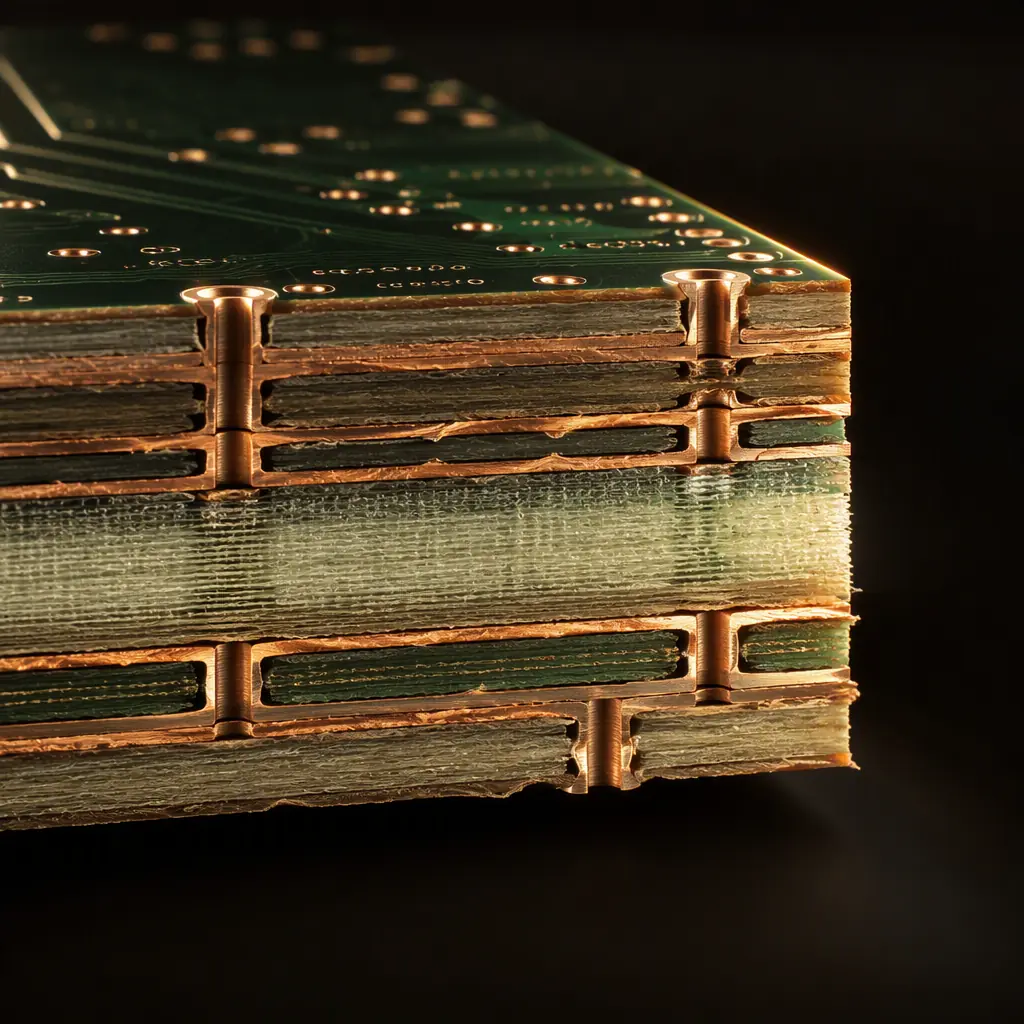
For HDI stackups, a microsection check confirms blind/buried via registration and copper plating thickness in the barrel. This is the one test that proves the inner-layer connections exist. Our microsection analysis guide explains the acceptance criteria.
Boundary-Scan Test the Assembled Board
With JTAG on the board, a boundary-scan test can verify every net on the FPGA's pins — catching assembly faults that functional test would chase for hours. Combine it with the X-ray results for a complete BGA picture. Our test method comparison helps you choose the right mix for your volume.
Summary: Power First, Signals Second, Assembly Third
An FPGA board works when three systems are designed in order: the power delivery network (rails, sequencing, decoupling, planes), the signal network (stackup, impedance, routing discipline), and the assembly network (fanout, stencil, X-ray, test access). Every one of these is decided before the first route is placed — which is exactly why talking to your manufacturer at schematic stage pays for itself.
At Huaxing PCBA, we manufacture FPGA boards up to 32 layers with HDI microvias, ±5% impedance control, and BGA placement down to 0.3 mm pitch. Our DFM review flags stackup, fanout, and testability issues before tooling. Read our stackup guide to prepare your design, or send your files for a free DFM review and quote.
