
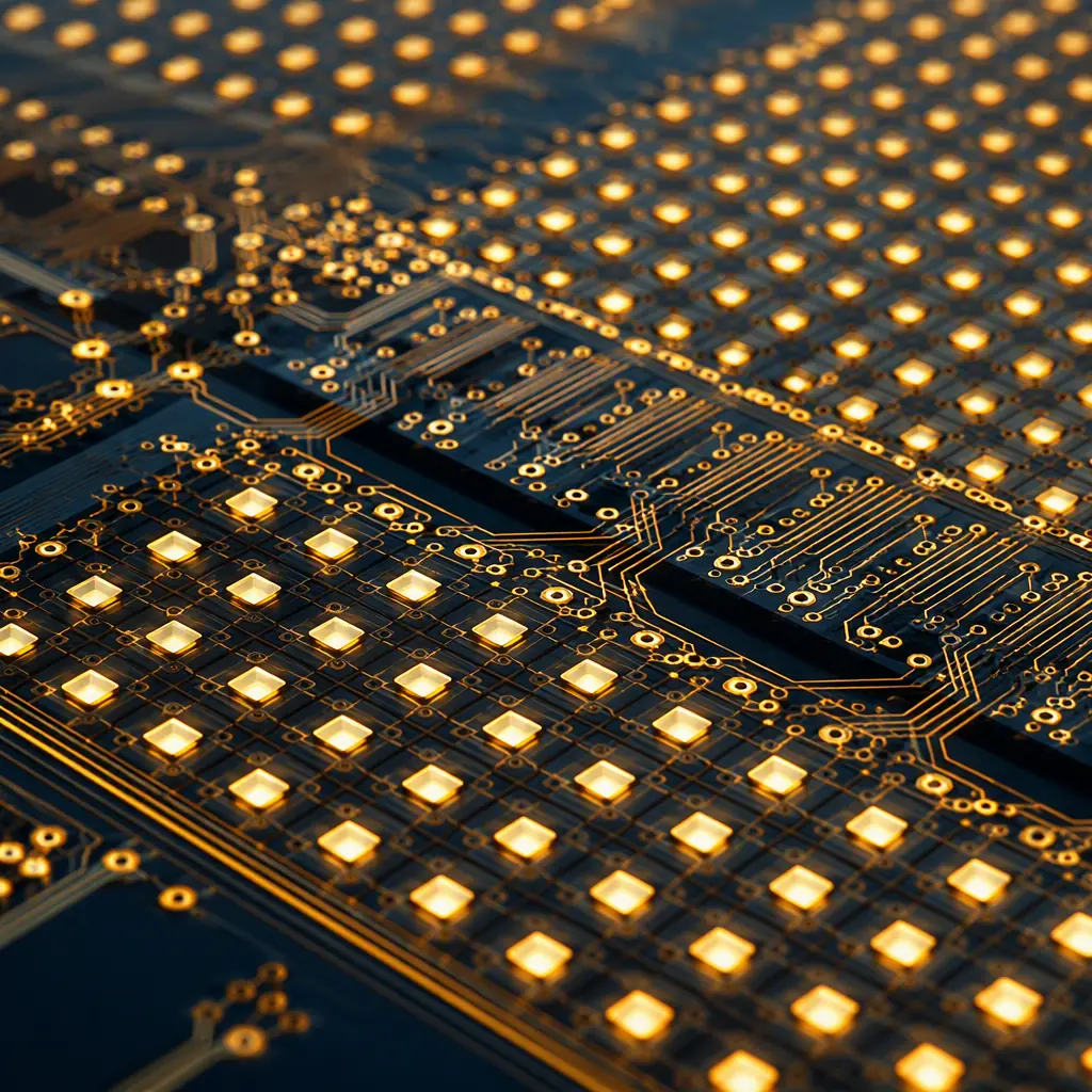
MicroLED is the display technology that keeps threatening to replace OLED. Each pixel is an inorganic gallium-nitride LED so small that a full 4K panel carries around 8.3 million of them. Unlike OLED, they are inorganic and do not burn in, and they can be driven to much higher brightness for outdoor and automotive use. The catch is not the LED. It is the backplane that has to route power and drive signal to millions of tiny pixels, and then get rid of the heat.
Huaxing PCBA builds boards down to 3/3 mil line and space, and to 32 layers, so micro-pitch and dense HDI are squarely within our range.
MicroLED vs OLED vs LCD, Why the Board Is Different
To design the driver board you have to understand what each display type demands of the substrate, because the backplane work is not the same.
LCD, The Easy but Old Backplane
LCD relies on a backlight and a liquid-crystal shutter. The board mostly drives row and column lines and a backlight, with relatively relaxed pitch. It is the least demanding, but also the least bright and the most prone to motion blur.
OLED, Self-Emissive but Organic
OLED is self-emissive and thin, and it is driven through a backplane that is typically a TFT array rather than a PCB. Its weakness is lifetime and burn-in, because the organic emissive material degrades over time.
MicroLED, Inorganic, Bright, and Harsh
MicroLED is inorganic and self-emissive, so it does not burn in and it can be very bright. The trade-off is that driving millions of tiny LED pixels demands a high-density backplane with fine pitch, and the aggregated heat has to be managed. See our LED PCB guide for the material choices.
Micro-Pitch Routing and Ultra-Fine HDI
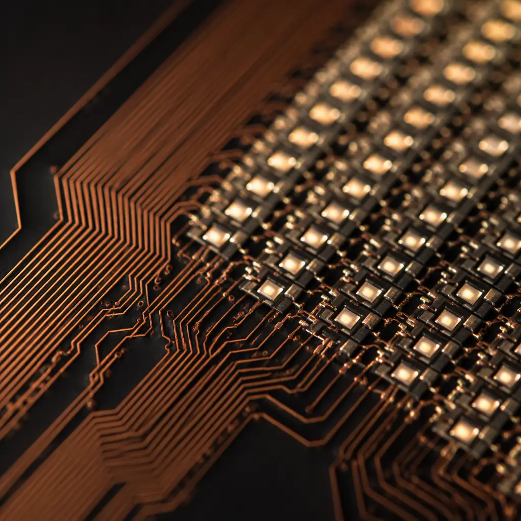
The backplane must route drive current and data to a very fine array. This is where the board fabricator's capability is tested hardest.
Fine Trace and Space at the Pixel Level
At high pixel pitches, the copper traces that fan out to the LED pads must be very fine. Depending on the pitch, we are talking 20-50 µm copper, well below the 3/3 mil Huaxing can do. See our manufacturing tolerances guide for what is achievable at each copper weight.
HDI and Microvia Stackup
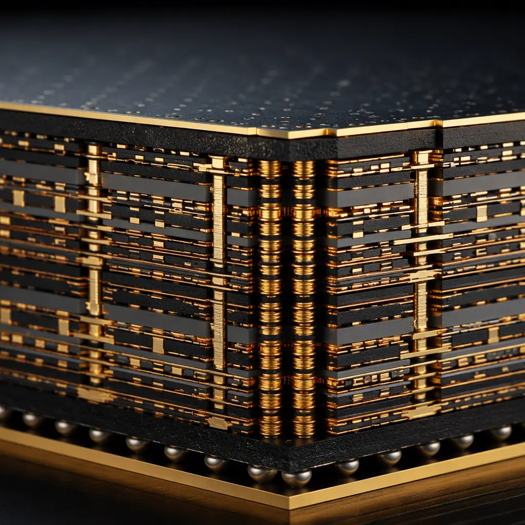
The backplane needs multiple routing layers to fan out millions of pixels and the driver data, so a dense HDI stack with microvias is standard. See our HDI technology guide and our microvia reliability guide.
Passive vs Active Matrix Drivers
At extremely high pitch, manufacturers move to active-matrix backplanes with TFT-like or transistor-in-panel drive. At larger pitch, the backplane uses a simpler passive or direct-drive approach. The choice changes the board's routing complexity, and it is set by the pixel pitch.
| Attribute | Typical MicroLED Requirement | Design Note |
|---|---|---|
| Pixel pitch | 10 – 500 µm | Sets trace and pad resolution |
| Trace width | 20 – 50 µm | Ultra-fine copper for fan-out |
| Layer count | 8 – 32 | Dense routing and reference planes |
| Solder mask | High-contrast / matte | Avoids glare from the LED backplane |
| Surface finish | ENIG / ENEPIG | Planar, solderable, flat contacts |
Thermal Design for a Bright, Dense Backplane
MicroLEDs are more efficient than older displays, but they are packed very densely and can run bright, which means the backplane has to conduct heat out efficiently.
Heat Spreading Through the Backplane
The aggregated heat from tens of thousands of little LEDs has to spread across the backplane and into a heat sink. Thick copper, thermal vias and careful placement of the hot rows all help. See our thermal management guide and our heavy copper guide.
Driving Current Without Voltage Drop
Each LED is a current-driven device, and the drive current has to reach the pixel without an excessive voltage drop across the fine trace. This limits trace length, forces wider power traces, and means a careful grounding scheme. See our trace width and current capacity guide.
Surface Finish and Solder Mask
The finish has to be flat and solderable for the tiny LED contacts, while the solder mask must be matte and non-reflective so it does not cause glare. See our surface finish guide and our solder mask guide for the choices.
Assembly and Inspection of a Micro-Pitch Display Board
Handling a micro-pitch backplane during assembly is as demanding as manufacturing it.
Fine-Pitch SMT Assembly
The driver ICs and the LED contacts are fine-pitch, so the SMT process has to place small components accurately. See our fine-pitch SMT guide and our assembly process guide for the approach.
AOI and X-Ray Inspection
The fine pitch and high density mean visual inspection alone is not enough. Automated optical and X-ray inspection catch defects at the pad and via level. See our inspection methods guide and our ATE testing guide.
Handling and Cleanliness
Display backplanes are sensitive to contamination and static. Controlled handling, ESD control and final cleaning are all part of a reliable build. See our ESD control guide and our cleaning guide.
Summary, Building a MicroLED Backplane
A microLED display backplane is a demanding mix of ultra-fine copper, dense HDI, and careful thermal design. Push the pitch as far as your process allows, use a well-planned HDI microvia stackup, and give the power and thermal paths the copper they need. Then assemble the fine-pitch parts with tight process control and inspect them with AOI and X-ray.
At Huaxing PCBA we build 2-32 layer boards down to 3/3 mil on 8 SMT lines, with ISO 9001 and UL certified quality and IPC Class 2/3 acceptance. We offer a free DFM review on the pitch, stackup and thermal plan of your microLED or display backplane, so it releases cleanly. Send your files for a quote or talk to an engineer about your display board.
