
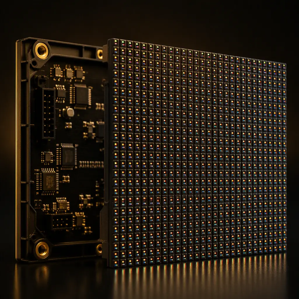
A direct-view LED video wall is not a screen. It is a grid of independent LED modules, each one a PCB carrying hundreds of surface-mount LEDs and the driver electronics that light them. The PCB is the display: its copper carries the current that sets brightness, its layout decides refresh rate and scan artifacts, and its thermal design determines whether the panel drifts in color after an hour of full-white output. For buyers specifying modules, understanding these board-level decisions is the difference between a wall that looks uniform for years and one that develops mura, dead rows or a hot corner after six months.
This guide covers the engineering decisions behind a video wall module, pixel pitch and module architecture, common-cathode versus common-anode power, driver IC layout, copper weight, and the manufacturing tolerances that matter when you panelize and assemble these boards at volume. Huaxing PCBA manufactures and assembles LED display modules from P0.9 fine-pitch indoor walls to P6+ outdoor cabinets, and this is the design guidance our DFM engineers apply to every display order.
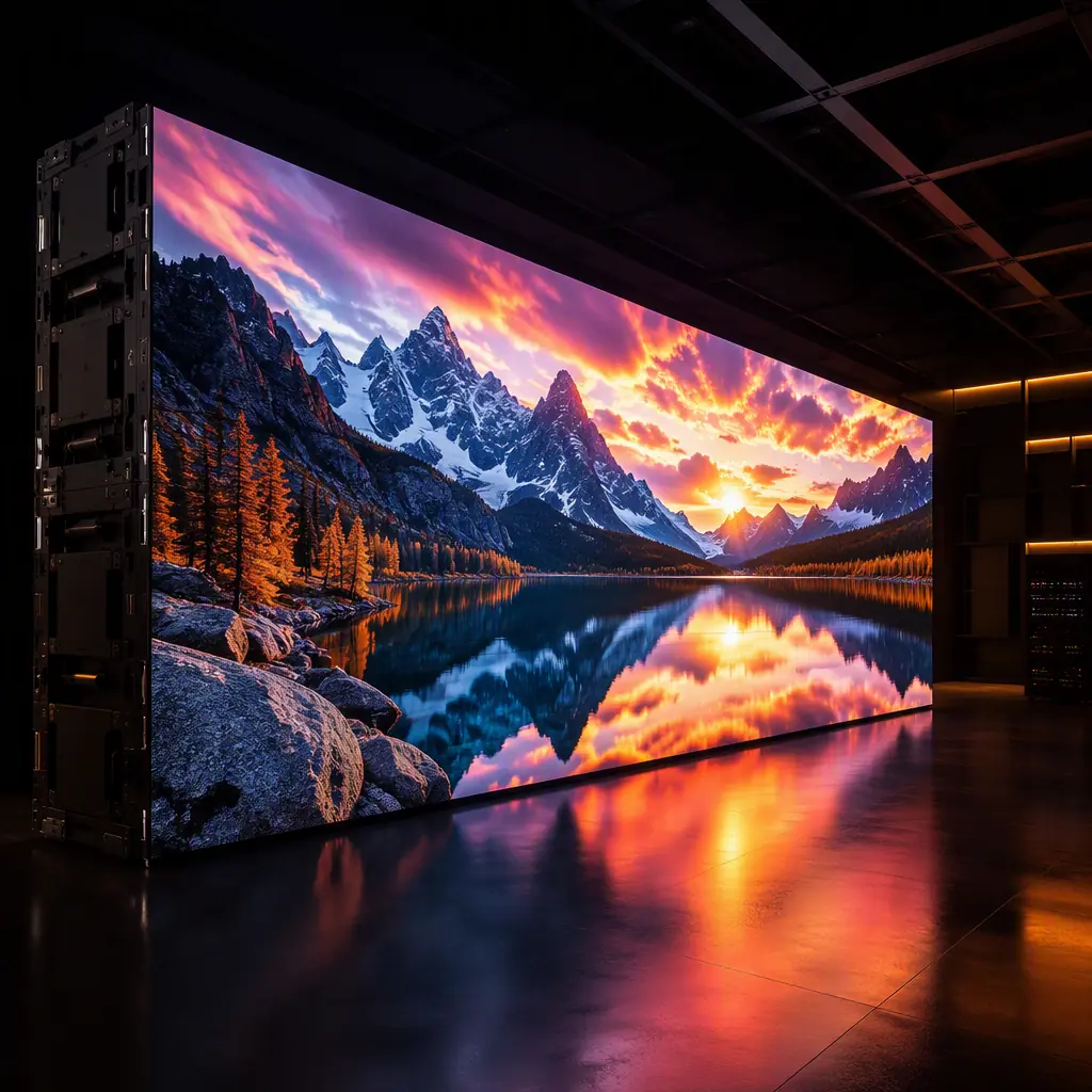
How a Video Wall Module Is Built, Architecture and Scan
A video wall module starts with a PCB panel, typically 320 × 160 mm for indoor modules or 500 × 500 mm for outdoor cabinets. The PCB carries the LEDs on the front and the driver ICs, connectors and decoupling on the back, or all on one side for smaller pitches. The key architectural decision is the scan configuration: how many LED rows share one driver channel.
| Parameter | Indoor Fine Pitch (P0.9–P1.8) | Indoor Standard (P2.0–P3.9) | Outdoor (P4–P10) |
|---|---|---|---|
| Typical module size | 320 × 160 mm | 320 × 160 mm | 500 × 500 mm (cabinet) |
| Scan ratio | 1/32 – 1/60 | 1/16 – 1/32 | 1/4 – 1/8 |
| LED package | 1010 / 1515 | 1515 / 2020 | SMD 2727 / DIP |
| Driver channels | 16 – 48 ch per IC | 16 ch | 16 ch |
| Typical refresh | 1920 – 3840 Hz | 1920 – 3840 Hz | 1920 – 3840 Hz |
The scan ratio directly shapes the PCB layout. At 1/32 scan, each driver channel services 32 rows of LEDs, so the row-select transistors, current sinks and the trace fan-out between driver IC and LED pads dominate the routing. At 1/4 scan (outdoor), the current per channel is much higher and the board becomes a power-routing problem before it is a logic-routing problem. Understanding which regime your design lives in tells you what the PCB actually needs, this parallels the design decisions covered in our LED PCB manufacturing guide, but display modules push current density and uniformity much harder than lighting boards.
Common-Cathode vs Common-Anode: The Power Architecture Decision
The single biggest electrical decision on a video wall module is whether the LEDs share a common cathode or a common anode. It changes the voltage rails, the driver IC choice, the copper routing and the thermal behavior of the whole panel.
Common-anode (CA), the traditional, simple rail
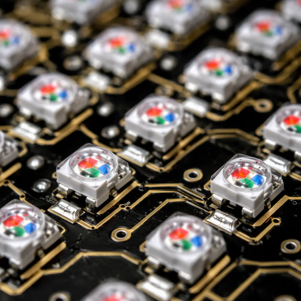
All LEDs share a common positive rail (typically 5 V), and the driver ICs sink current from each LED's cathode to ground. One rail, simple routing, mature driver ecosystem. The cost is efficiency: a red LED forward voltage is ~2.0 V, green ~3.0 V and blue ~3.2 V, so driving them all from 5 V wastes 1.8–3 V as heat in the driver and the LED. On a large wall running 24/7, that wasted power is real money and real heat.
Common-cathode (CC), matched rails for efficiency and thermals
Common-cathode modules split the LEDs by color and feed each color its own rail: typically 3.8 V for blue/green and 2.8 V for red. Each LED sees a rail only slightly above its forward voltage, so far less energy is dumped as heat. CC modules run measurably cooler at the same brightness: typically 10–15°C lower LED temperature at full white on comparable designs, which slows LED lumen decay and reduces color drift. The cost is a second power rail, more complex routing and driver ICs that support split-supply operation.
Which one to specify
For fine-pitch indoor walls (P1.8 and below) and any application running high brightness for long hours, control rooms, broadcast studios, retail, common-cathode is now the default because the thermal budget dominates reliability. For outdoor high-pitch cabinets where the driving voltage and current are lower per LED and the enclosure handles cooling, common-anode remains viable and cheaper. The specification decision belongs in the RFQ. It is exactly the kind of detail a buyer should pin down before quoting, alongside the points covered in our PCB specification and RFQ guide.
Key Takeaway: Common-cathode is the efficiency and reliability play for fine-pitch and high-brightness displays; common-anode is the cost play for high-pitch outdoor cabinets. The PCB copper and stackup follow the decision, not the other way around.
Copper Weight, Stackup and Current Routing
A video wall module is a power board wearing a display costume. At full white, a 320 × 160 mm indoor module draws roughly 3–5 A, and an outdoor P6 cabinet can draw 8–15 A through the power input connectors. That current has to reach hundreds of LEDs with a voltage drop small enough that the first and last LED see nearly identical drive conditions, otherwise the panel shows a visible brightness gradient from the power input side to the far edge.
Copper weight: 2 oz is the floor for display modules
Standard signal boards run 1 oz copper. Video wall modules typically require 2–4 oz on the power layers, with the heaviest copper under the power input zone and the row-drive return paths. At 3 A through a 0.5 mm trace, a 1 oz trace rises visibly in temperature and drops too much voltage; 2 oz copper roughly halves both. The trade-off is etch tolerance and minimum feature size. Heavier copper limits how tight the fine-pitch LED fan-out can be, which is why fine-pitch modules balance a 2 oz power plane with 1 oz signal layers. Copper weight selection rules for high-current zones are covered in our PCB copper weight guide.
Stackup: 4-layer is typical, 6-layer for fine pitch
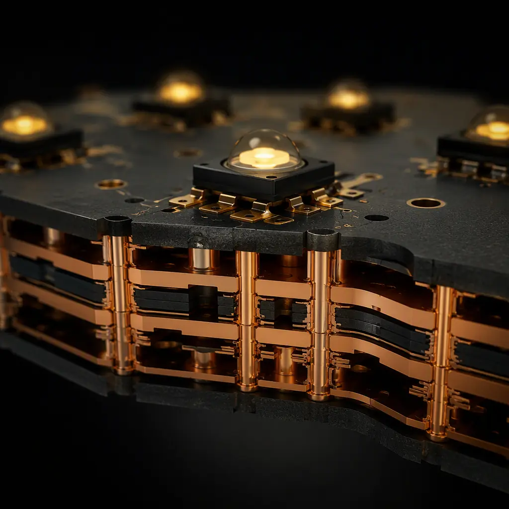
A standard display module is a 4-layer board: top signal (LED pads and fan-out), inner power split (VCC/rail planes), inner ground, bottom signal (driver ICs, connectors). Fine-pitch modules (P1.2 and below) move to 6 layers because the LED fan-out and the driver routing can no longer share one outer layer without via congestion. High-Tg FR-4 (TG150–170) is standard. The module sits in an enclosure with limited airflow, and the board itself is the main heat spreader. Stackup planning for dense boards is covered in our PCB stackup design guide.
Uniformity-driven layout rules
Every LED pad should see the same trace length and resistance back to its driver channel. That means mirrored routing, balanced fan-out and generous via stitching between the power planes. A ±5% channel-current difference that is invisible on a 10 mm pitch sign becomes a visible brightness band on a P1.5 wall. The impedance and routing discipline is the same family of rules described in our impedance control guide, applied here to DC resistance rather than AC signals.
Thermal Management: The Board Is the Heat Sink
LEDs convert roughly 70–80% of input power to heat. On a video wall module there is no fan per module and the enclosure airflow is limited, so the PCB is the primary thermal path: heat conducts from the LED pad, through thermal vias, into the copper planes, and out to the module frame or backplate. Three things determine whether that path works.
| Thermal Element | What It Does | Typical Spec |
|---|---|---|
| Thermal vias under LED pads | Conduct heat from LED junction to inner planes | 0.2–0.3 mm, filled or tented, 4–9 per pad |
| Copper plane area | Spreads heat laterally across the module | ≥60% plane coverage on inner layers |
| LED pad design | Maximizes solder contact area and thermal path | Pad matched to LED package thermal pad |
The failure mode to design against is thermal mura: LEDs at the center of a module run hotter than those at the edge, lose brightness faster, and the wall develops a visible grid of darker modules over time. Keeping junction temperature below the LED vendor's rating: typically 85–100°C for SMD display LEDs, with margin is the reliability target. The full toolbox, thermal vias, plane design, substrate selection, is covered in our PCB thermal management guide; display modules just apply it at higher density than most boards.
Factory Reality: A 500 × 500 mm outdoor module in full sun absorbs solar load on top of its own electrical heat. Outdoor cabinet designs routinely derate brightness and add backplate cooling for this reason. The PCB thermal path is designed for the worst case, not the lab case.
Driver IC Placement and Signal Integrity
The driver ICs sit on the back side (or on the same side for very fine pitch), each driving 16–48 LED channels through a constant-current output. Placement and routing around these ICs decide scan quality and noise.
Keep the constant-current loop tight
The sense resistor, decoupling cap and driver output form a high-frequency current loop. A tight loop means stable channel current; a wide loop means crosstalk between channels and visible flicker at low brightness. Decoupling: 0.1 µF + 1 µF per driver IC is the baseline, with a bulk cap per module section.
Row-select and scan timing routes
The scan signals (row-select lines, clock, latch) run at the module's scan frequency, and skew between them shows up as a visible diagonal banding artifact. Route them as a matched group with controlled length, away from the high-current LED return paths. The EMC and noise discipline for this mixed power/digital board follows our EMI/EMC design guide.
Connector and cascade design
Modules daisy-chain power and data through board-to-board or HUB connectors. The data connectors (typically 16–26 pin) carry the scan and clock signals across modules, so their placement defines the cascade direction and the routing fan-out on the board. Power connectors need the copper and via budget described above. A connector rated for 5 A that feeds a 10 A cabinet input is a field failure waiting to happen.
Manufacturing Tolerances That Determine Display Quality
Two modules from the same design can look different on a wall if the manufacturing tolerances drift. The tolerances that matter for display quality are tighter than for ordinary electronics:
LED placement accuracy
On a P1.5 module the LED pitch is 1.5 mm and the placement tolerance budget is roughly ±0.05 mm per LED. Cumulative placement error between adjacent modules is what creates visible seams and pixel misalignment at the module boundary. This is decided by the SMT process, stencil, placement and reflow, covered in our SMT stencil design guide.
Board flatness and module geometry
Module-to-module gaps must be uniform or the wall shows dark grid lines. Board flatness (warpage) after reflow is the enemy, a bow of 0.5% of the module length is already visible at the seams. Warpage control, from stackup symmetry to panel design, is covered in our PCB warpage guide.
Panelization for display modules
Display modules are panelized for SMT and depanelized before final assembly. The scoring or routing strategy must not stress the board edge where LEDs sit. Depanelization methods and their edge-stress profiles are compared in our depaneling methods guide.
Testing a Video Wall Module Before It Ships
Display modules get electrical test plus a lighting test that ordinary boards never see. Beyond standard AOI and functional test, display manufacturers run:
- Aging test . Full-white burn-in for 48–72 hours to catch early LED failures and stabilize brightness before calibration.
- Brightness/color uniformity scan . Camera-based measurement of every module against the target white point and brightness bin.
- Scan artifact check . Low-brightness and grayscale ramps to expose flicker, banding and ghosting.
AOI and X-ray catch the assembly defects, solder bridges under fine-pitch LEDs, missing components, cold joints, before the lighting test. The inspection methods are the same ones covered in our AOI vs X-Ray vs SPI inspection guide, applied at tighter criteria for display work.
Summary: The Video Wall Module Specification Checklist
When you specify a video wall module PCB, pin down nine things: pixel pitch and scan ratio, module size, common-cathode or common-anode architecture, copper weight (2 oz minimum on power layers), stackup (4 or 6 layer), TG rating (≥150), thermal via strategy under LED pads, LED placement tolerance (±0.05 mm at fine pitch), and the test protocol (aging, uniformity scan, AOI/X-ray). Every one of these is a manufacturing spec, not a marketing bullet. Which is exactly why they belong in the RFQ and the DFM review.
Huaxing PCBA manufactures and assembles LED display modules from P0.9 to P10+, with 2–4 oz copper, common-cathode support, and camera-based uniformity testing on the assembly line. Read our panelization guide to see how display modules are panelized for cost, or send our engineering team your display design for a free DFM review and quote within 24 hours.
