
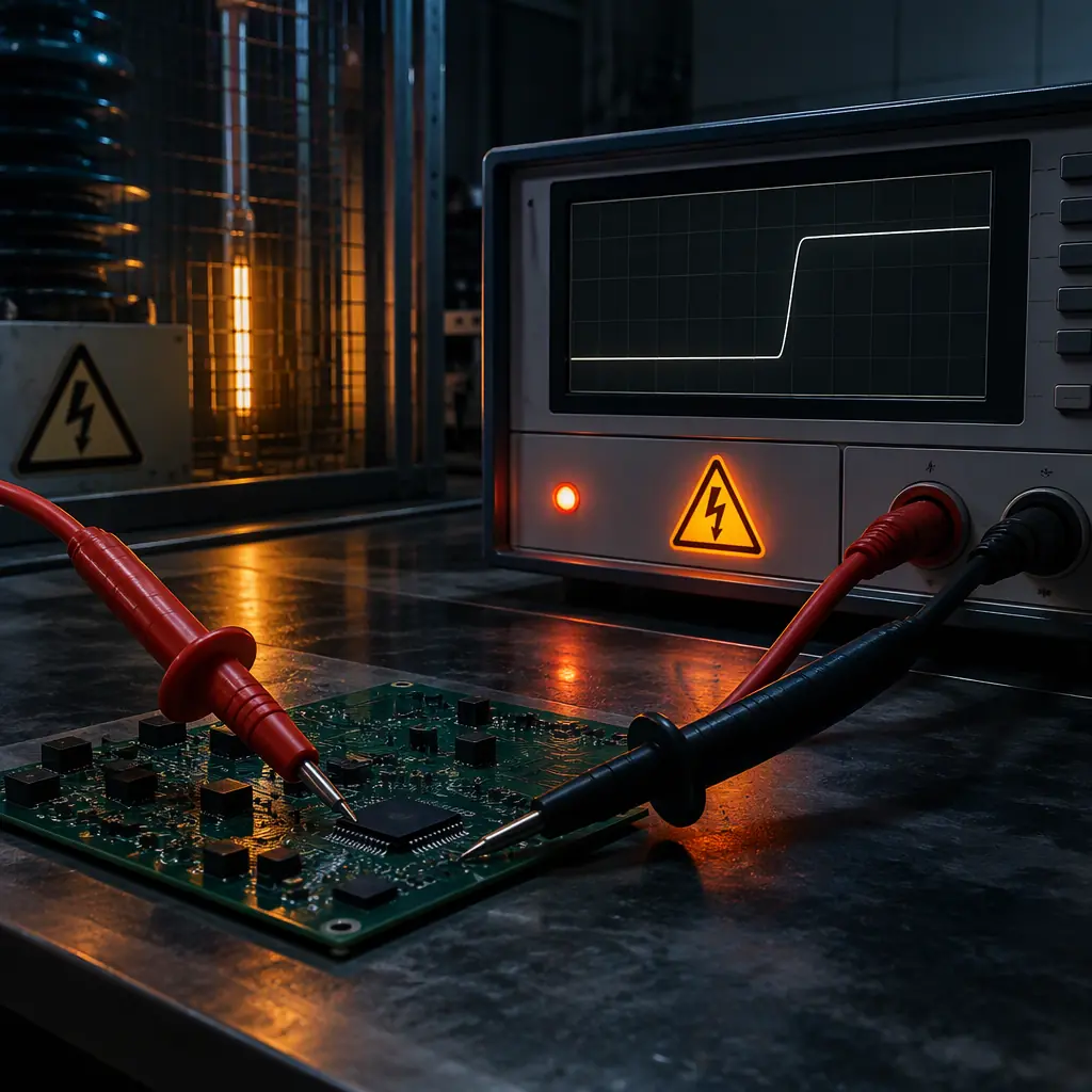
The high-potential test — hi-pot for short — is one of the most frequently requested and most frequently misunderstood tests in electronics. It is often assumed to be a functional test, or a test of the assembly as a whole. It is neither. A hi-pot test applies an elevated voltage between two points that should be isolated and measures whether any current leaks across the gap. It says nothing about whether the circuit works. What it proves is narrower and more important: that the insulation separating two conductors will not break down under stress. For any product with mains voltage, a high-voltage rail, or a safety barrier between a user and live circuitry, that is the single most safety-relevant thing a test can establish.
This guide covers the test itself: what hi-pot does and does not prove, how the test voltage is derived, how the setup — ramp, dwell, trip current — changes the result, what the three failure modes mean, how a hi-pot test can damage the assembly it is meant to protect, and how to specify it in a purchase order. It is the test-side companion to our high-voltage PCB design guide, which covers creepage and clearance in the layout, and it sits alongside PCB testing methods for the wider test programme.
At Huaxing PCBA we run hi-pot testing as part of the test programme for assemblies with isolation requirements across 8 SMT lines under IATF 16949 and ISO 9001, with the test voltage, ramp and trip limits written into the test specification per programme rather than left to the bench. The parameter set is documented because a hi-pot result is only meaningful against stated conditions.

What Hi-Pot Proves — and What It Does Not
Keeping hi-pot in its proper place prevents both over-reliance and misplaced rejection.
What it proves. Hi-pot proves that the insulation between the stressed points can withstand the applied voltage for the duration of the test without leaking more than the trip current, and without breaking down. It is a check on the dielectric strength of the insulation — the board material, the spacing, the coating, the air gaps — and on the integrity of the isolation barrier. For a product where a user or a downstream circuit must be separated from a hazardous voltage, this is the direct evidence that the barrier holds.
What it does not prove. Hi-pot does not test whether the circuit functions, whether components are correctly placed or oriented, whether solder joints are good, or whether the firmware is correct. A board with a completely absent functional component can pass hi-pot with flying colours, because the component is not part of the insulation being tested. It also does not prove long-term reliability: passing a hi-pot test means the insulation held for the few seconds of the test, not that it will hold for the life of the product. It is a screen for gross defects and a proof of a design property, not a reliability demonstration — which is why it complements, rather than replaces, the other tests in the programme. See PCB testing methods for how the pieces fit together.
Key Takeaway: Hi-pot is an insulation test, not a functional test. It proves the isolation barrier holds under the applied voltage — nothing more and nothing less. Expect it to catch gross insulation defects and to prove a safety property; do not expect it to catch a wrong component or a dry joint.
How the Test Voltage Is Derived
The test voltage is not arbitrary and should not be guessed. For equipment insulation in most product safety standards, the routine test voltage is defined relative to the working voltage the insulation will see in service, using a formula of the general form:
Vtest = 2 × Vworking + 1000 V
with variations by standard and by the class of insulation. The logic of the formula is that the test must exceed the working voltage by a margin large enough to catch marginal insulation — the factor of two stresses the barrier well beyond normal operation — plus a fixed offset that provides a floor for low-voltage circuits and accounts for the difference between a short routine test and a continuous service condition. Some standards use different multipliers or add-offs, and some applications specify the test voltage directly. Always take the value from the product standard that applies to the end product, not from a generic rule of thumb.
Two consequences follow, and both matter to a buyer specifying the test.
First, the test voltage depends on where in the product the insulation sits. A barrier between a mains input and a low-voltage secondary is stressed at a much higher voltage than a barrier between two low-voltage domains on the same board. The duty of the barrier determines the test value, and a specification that names a single test voltage for the whole assembly without reference to the barrier under test is not a specification.
Second, the test voltage is applied for a defined time — the dwell — and that time differs between a routine production test and a type test. A routine test on every unit is shorter than the qualification test on a sample, because the wear of repeated stress accumulates. Applying a type-test voltage and duration to every unit in production over-stresses the insulation and can create the very failures the test is meant to prevent. This is a common error when a specification is copied from a qualification report directly into a production purchase order.
The Setup: Ramp, Dwell and Trip Current
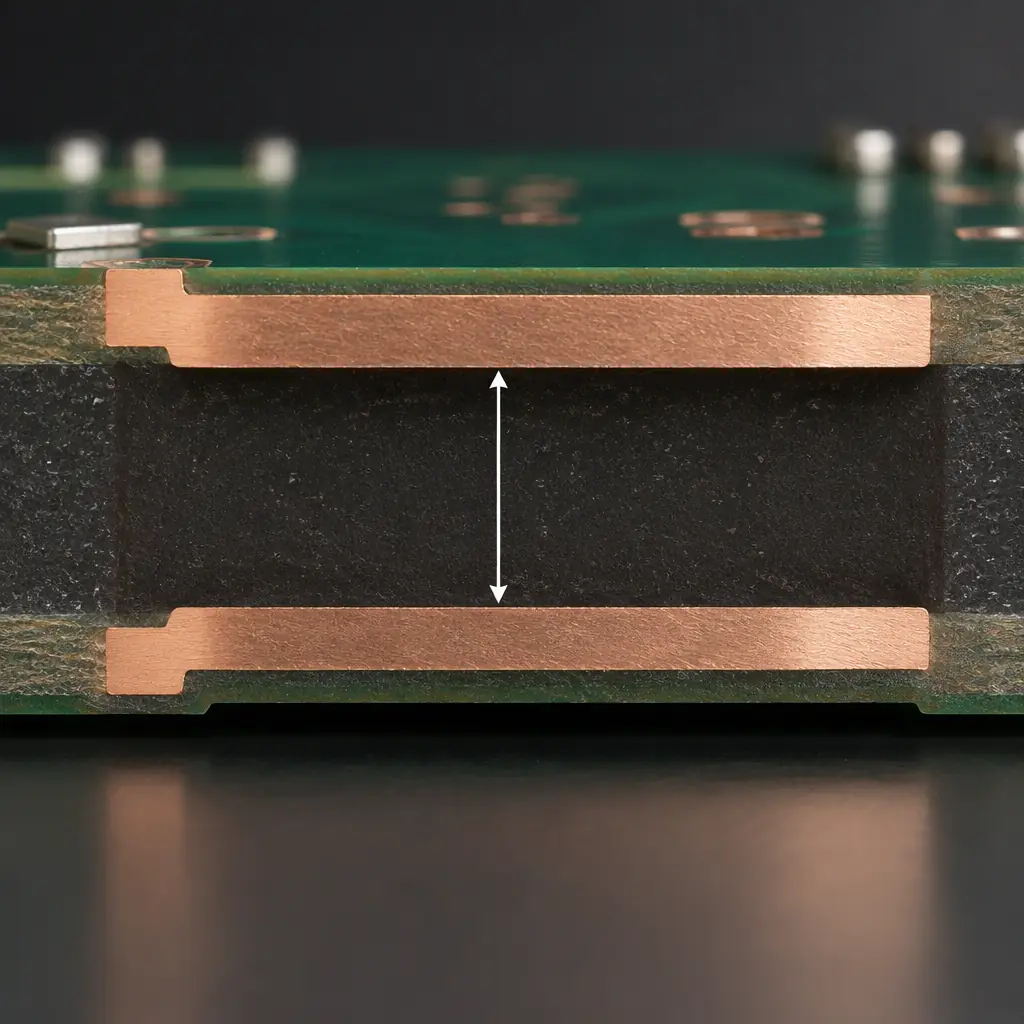
The three setup parameters decide what the test actually stresses and how a pass is judged. Set them wrong and a good board fails, or a bad board passes.
| Parameter | What it controls | Effect if set wrongly |
|---|---|---|
| Ramp rate | How fast the voltage climbs to the test value | Too fast stresses the insulation transiently and can arc; too slow wastes cycle time |
| Dwell time | How long the test voltage is held | Too short and a marginal defect escapes; too long over-stresses good boards |
| Trip current | The leakage level at which the instrument judges a failure | Too low and normal capacitive/creepage current fails good boards; too high and small breakdowns pass |
| Stressed points | Which nets are connected to high and low | Wrong points test the wrong barrier, or stress components not meant to see the voltage |
| Discharge | Safe removal of stored charge after the test | Skipping it leaves stored voltage in the board and in the operator's hands |
The ramp matters because insulation behaves differently under a sudden step than under a gradual rise; a step can cause a transient breakdown that a proper ramp would avoid, and the standard methods specify a controlled ramp for exactly this reason. The dwell is the defined stress window and must match the applicable test. The trip current is the trickiest: insulation is not a perfect open circuit, and at elevated frequency or across a large area a good barrier still passes a small leakage current, part of it capacitive and part of it surface creepage. Setting the trip current below that normal leakage fails good boards, and setting it far above lets a genuine partial breakdown through. The trip current belongs with the barrier being tested, not set to a single number for the whole assembly.
How the stressed points are chosen is as important as the voltage. The test must be applied across the barrier that actually provides the safety isolation, and only across it. A test applied across the wrong points may leave the real barrier untested, or may stress a component that is not rated for the voltage and damage it — a real risk discussed below. The test points should be defined in the test specification and, where possible, brought out to test pads so the fixture does not have to probe live circuitry. See PCB design for testability for how test access is built in at design time.
Reading a Failure: Breakdown, Leakage or Setup Artefact
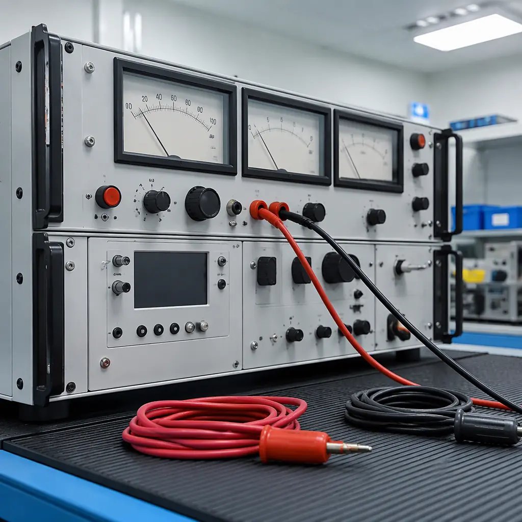
A hi-pot failure is not automatically a defect. Three distinct things can trip the instrument, and only one of them is the insulation failing.
Genuine breakdown
A true dielectric breakdown shows as a sudden, often large increase in current at a reproducible voltage — the insulation has given way and the barrier is gone. This is the failure the test exists to find: insufficient spacing, a conductive contamination path, a crack, a coating void or a punctured layer. A genuine breakdown usually reproduces on a repeat test at the same or a lower voltage, and the part is scrap. See high-voltage design for the spacing rules that prevent it and ionic contamination control for the contamination path.
Real leakage over a marginal barrier
A barrier that does not break down but leaks more than the trip current has a marginal insulation condition — often surface contamination, moisture or an insufficient coating. This is a genuine reject, but of a different kind: the barrier is present but compromised, which is exactly the marginal condition that fails later in the field. It is often intermittent and moisture-sensitive, and it is the reason the test environment — particularly humidity — must be controlled for the result to be meaningful.
Setup artefact
The most common reason a good board appears to fail is the test setup, not the board. A trip current set below the normal capacitive leakage, a probe contacting a coating rather than a pad, residual flux or handling contamination bridging a surface path, moisture on the board, or a fixture that stresses the wrong points all produce failures that disappear when the setup is corrected. A board that fails should be re-tested after cleaning and drying, with the setup verified, before it is scrapped. Misreading an artefact as a defect destroys good product and hides the real cause.
Procurement tip: When a supplier reports hi-pot failures, ask which of the three it was, and how it was distinguished. A supplier who retests after cleaning and setup verification, and only then scraps, understands the test. A supplier who scraps on the first trip, without separating artefact from defect, is either wasting yield or — worse — passing marginal boards by loosening the limit until nothing fails.
The Test Can Damage What It Tests
This is the point most often missed when hi-pot is specified casually: the well-intentioned safety test can damage the assembly. Hi-pot applies a voltage chosen to stress insulation, and that voltage is applied across whatever lies between the two test points — not only the insulation barrier, but any component, coating or structure bridged by those points. Components with a rated voltage below the test voltage can be degraded or destroyed by the test, and repeated routine testing accumulates stress on the insulation itself. Coating and potting materials can develop local breakdown paths under repeated stress that were not there before.
The implication for a specification is that the test must be scoped: the test voltage, the dwell and the stressed points must be chosen so the barrier is stressed and nothing else is over-stressed. Where components sit across the barrier, either they must be rated for the test voltage, or the test must be designed to exclude them — for example by testing before those components are fitted, or by testing a sub-assembly rather than the finished unit. A hi-pot test that stresses the correct barrier and nothing else is safe; one that applies a blanket high voltage across a populated board is not. See EMC and compliance for how the safety tests fit with the wider compliance programme, and thermal interface materials for the material breakdown considerations that share the same physics of voltage stress across a gap.
Specifying Hi-Pot in the Purchase Order
Hi-pot is a test whose result is meaningless without its conditions. The purchase order has to carry all of them.
Name the barrier and the test points
State which isolation barrier is under test and which nets are connected to the high and low sides of the instrument. The barrier is the thing being proven; a test that does not name it does not prove it.
State the test voltage, the standard it comes from, and whether it is a routine or type test
Give the test voltage and cite the product standard and clause it derives from. Make explicit whether the value is the routine production test or the type test, because applying the type-test value to every unit over-stresses the board. See the specification and RFQ guide for how the clause sits with your other requirements.
State ramp, dwell and trip current
Name the ramp rate, the dwell time and the trip current. These three set what the test stresses and how a pass is judged; without them, two suppliers can both claim to have "passed hi-pot" while testing different things.
State the disposition rule for a failure
Agree in advance that a failure is to be distinguished as breakdown, leakage or artefact before disposition, and that a retest after cleaning and setup verification is required before any part is scrapped. This protects your yield and your supplier's, and it is the difference between a controlled test and a coin toss. See PCB outgoing quality control for how hi-pot sits in the shipped-goods control, and quality dispute resolution for how to handle a disagreement about a result.
Summary: An Insulation Test, Specified in Full
Hi-pot is a narrow, powerful test. It proves that an isolation barrier withstands an applied voltage — and nothing about whether the circuit works. The test voltage is derived from the working voltage and the applicable product standard, not guessed; the ramp, dwell and trip current decide what is stressed and how a pass is judged; and a failure is only a defect after breakdown, leakage and setup artefact have been told apart. Because the test stresses everything between the test points, not just the barrier, it must be scoped so it damages nothing. Specified in that full detail, hi-pot is one of the strongest safety controls a buyer can put on an order; specified as a bare voltage, it proves very little.
At Huaxing PCBA we run hi-pot testing for assemblies with isolation requirements as part of the documented test programme across 8 SMT lines under IATF 16949 and ISO 9001, with the barrier, voltage, ramp and trip limits written into the specification per programme. If your product has a safety barrier or a high-voltage rail, tell us the standard that applies and we will build the test specification around it. Send your Gerber and BOM and we will confirm the hi-pot parameters for your build and return a quote inside 24 hours, or talk to our test engineering team about an isolation requirement you are working through.
