
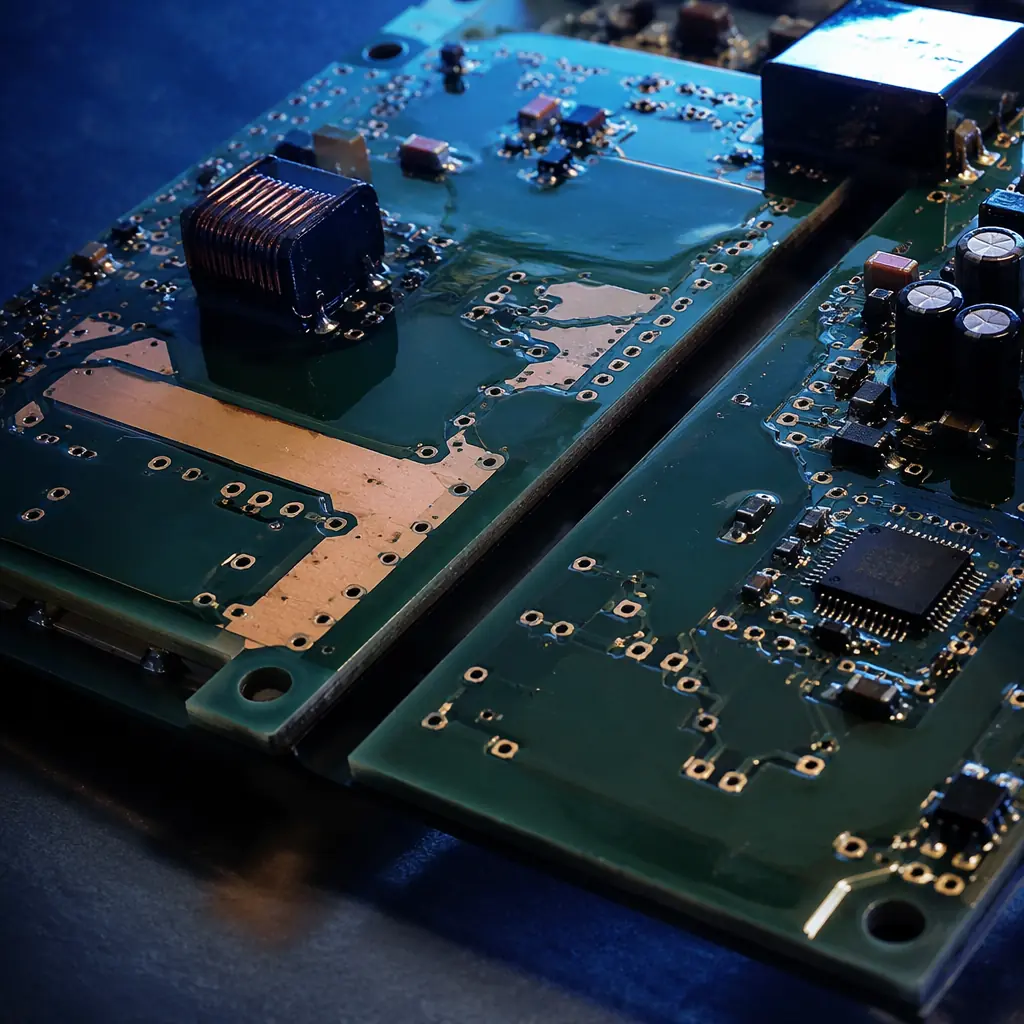
When your PCB carries 500V or more, standard FR-4 spacing rules stop being guidelines and become safety-critical engineering decisions. A 0.2mm trace gap that works flawlessly at 12V can arc across at 600V, destroying components and creating a fire hazard. High-voltage PCB design is not about adding extra margin, it's about understanding the physics of dielectric breakdown, creepage paths along contaminated surfaces, and the certification requirements that determine whether your product ships or gets rejected at compliance testing.
This guide covers the IPC-2221 voltage spacing requirements, the difference between creepage and clearance (and why confusing them causes field failures), how to select PCB materials with the right Comparative Tracking Index (CTI), and five layout rules proven across thousands of high-voltage boards manufactured at our IATF 16949 certified facility. At Huaxing PCBA, we process high-voltage PCBs from 2 to 32 layers with materials rated to 40kV/mm dielectric strength, serving EV charging, solar inverter, industrial VFD, and medical imaging customers across 30+ countries.
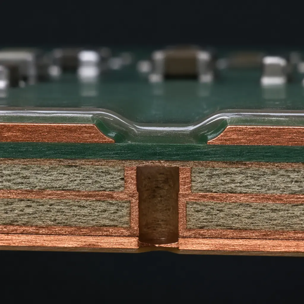
What Counts as "High Voltage" in PCB Design?
Industry standards don't use a single voltage threshold. The classification depends on which standard you're designing to, and getting this wrong at the schematic stage cascades into board respins and certification failures.
| Standard | Low Voltage | High Voltage | Notes |
|---|---|---|---|
| IPC-2221 | <100V (internal), <500V (external) | ≥100V internal, ≥500V external | Spacing tables split at these thresholds |
| IEC 60950-1 / 62368-1 | <60V DC, <42.4V AC peak | ≥60V DC / 42.4V AC | Safety Extra-Low Voltage (SELV) boundary |
| IEC 60664-1 | Depends on overvoltage category | Depends on rated impulse voltage | Used for mains-connected equipment (CAT II–IV) |
| UL 60950-1 | ES1 (<60V) | ES2 (60–250V), ES3 (>250V) | Energy Source classification |
For most PCB designers, the practical boundary is 500V peak. Below this, IPC-2221 spacing tables give adequate margins for clean, dry, indoor environments. Above this threshold, or any time your board connects to AC mains, you enter the world of creepage distance calculations, pollution degree classifications, and material CTI requirements. The applications that routinely cross this boundary include EV onboard chargers (400–800V), industrial VFD DC buses (560V), solar string inverters (600–1500V), and medical X-ray generator supplies (40–150kV with special isolation).
Creepage vs Clearance, The Distinction That Prevents Field Failures
These two terms are often used interchangeably by engineers who haven't designed for high voltage before, but they describe fundamentally different failure mechanisms, and IEC/UL standards treat them as separate requirements.
Clearance, The Shortest Path Through Air
Clearance is the line-of-sight distance between two conductive parts through air. It protects against transient overvoltage . The lightning strike, the switching surge, the ESD event. Air breaks down at approximately 3kV/mm at sea level under standard conditions, but this drops significantly at altitude (lower air density = easier breakdown). For a PCB operating at 1,000m altitude, the derating factor is approximately 0.89x; at 3,000m, it drops to 0.73x. Clearance requirements come from the expected transient overvoltage category (CAT II/III/IV), not the working voltage.
Creepage, The Path Along a Surface
Creepage is the shortest path along the surface of an insulator between two conductors. It protects against long-term tracking . The gradual degradation of the PCB surface when voltage stress, humidity, and contamination combine to form conductive carbon paths. A board that passes dielectric withstand testing in the lab can fail in the field after 6–12 months of dust accumulation and humidity cycling. Creepage requirements are calculated from the RMS working voltage, the pollution degree of the operating environment, and the Comparative Tracking Index (CTI) of the PCB base material.
Key Insight: The most dangerous failure mode in high-voltage PCBs is not dielectric breakdown, it's electrochemical migration (ECM). When moisture condenses on a contaminated PCB surface between two traces at different potentials, copper ions migrate from the anode to the cathode, forming conductive dendrites. This happens below the dielectric breakdown voltage and below the clearance arc-over threshold. Only adequate creepage distance, accounting for pollution degree, prevents it.
IPC-2221 Spacing Requirements by Voltage Level
The IPC-2221 standard provides the baseline conductor spacing table that most PCB designs reference. For high-voltage work, use Table 6-1 (electrical conductor spacing) with the B4 column for external conductors with permanent polymer coating, or the A5/A6/A7 columns depending on your specific application and altitude. Below are the key voltage-to-spacing mappings:
| Voltage (DC or AC Peak) | B1, Internal | B2, External, Uncoated | B4, External, Coated | Typical Application |
|---|---|---|---|---|
| 0–15V | 0.05mm | 0.1mm | 0.05mm | Digital logic, microcontrollers |
| 16–30V | 0.05mm | 0.1mm | 0.05mm | Analog sensor circuits |
| 31–50V | 0.1mm | 0.6mm | 0.13mm | Power-over-Ethernet (PoE) |
| 51–100V | 0.1mm | 0.6mm | 0.13mm | 48V battery systems, audio amps |
| 101–150V | 0.2mm | 1.25mm | 0.4mm | DC-DC converter primaries |
| 151–170V | 0.2mm | 1.25mm | 0.4mm | US mains rectified (120V AC → 170V DC) |
| 171–250V | 0.2mm | 1.25mm | 0.4mm | EU mains rectified (230V → 325V DC) |
| 251–300V | 0.2mm | 1.25mm | 0.4mm | PFC boost output stage |
| 301–500V | 0.25mm | 2.5mm | 0.8mm | 3-phase rectified bus, EV charger input |
| 501–600V | 0.5mm | 3.2mm | 1.0mm | EV traction inverter DC link |
| 601–800V | 0.75mm | 4.0mm | 1.25mm | 800V EV architecture, solar string inverters |
| 801–1000V | 1.0mm | 5.0mm | 1.5mm | Industrial VFD DC bus, 1500V solar |
Note that the B2 column (uncoated external) jumps dramatically above 500V. From 2.5mm to 5.0mm between 500V and 1000V. This is precisely why conformal coating (B4) is almost mandatory for production high-voltage boards: it more than halves the required spacing, enabling denser layouts without sacrificing safety. For a deeper understanding of coating options, see our conformal coating selection guide which covers silicone, acrylic, and parylene materials for high-voltage PCB protection.
Material Selection for High-Voltage PCBs
Not all FR-4 is created equal when voltage climbs above 500V. Two material properties dominate high-voltage PCB reliability: Comparative Tracking Index (CTI) and dielectric breakdown strength. Selecting the wrong grade of FR-4 for a 600V design can reduce creepage life by 10–100x compared to a properly specified high-CTI laminate.
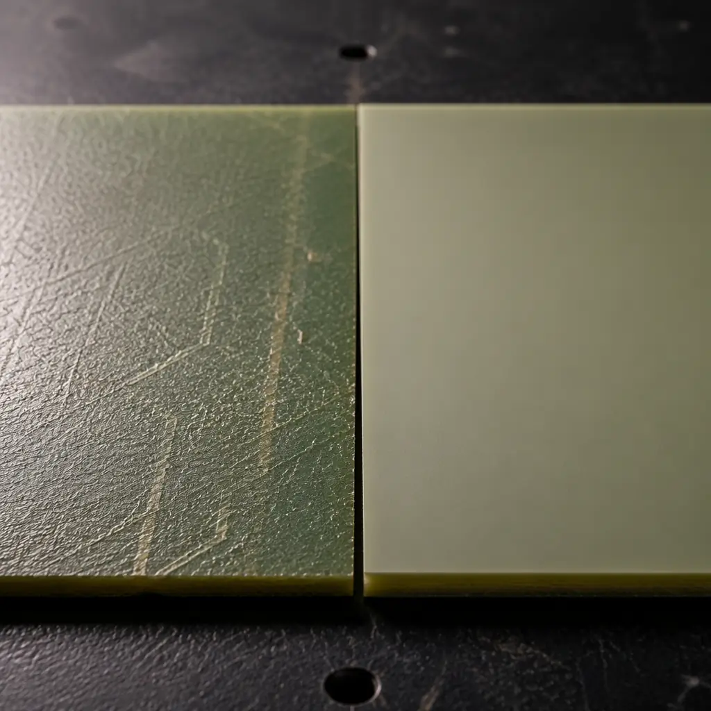
| Material | CTI (Volts) | PLC Rating | Dielectric Strength | Cost Multiplier | Best For |
|---|---|---|---|---|---|
| Standard FR-4 | 175–249V | PLC 3 | 20–30 kV/mm | 1.0x | ≤150V designs, non-safety-critical |
| High-Tg FR-4 (Tg 170°C+) | 200–300V | PLC 2–3 | 25–35 kV/mm | 1.2–1.4x | High-temp environments with moderate voltage |
| High-CTI FR-4 (CTI ≥400V) | 400–599V | PLC 1 | 30–40 kV/mm | 1.5–2.0x | 500–800V designs, Pollution Degree 2 |
| Polyimide | ≥600V | PLC 0 | 40–60 kV/mm | 3.0–5.0x | 800V+, flex/rigid-flex, aerospace |
| Ceramic-filled PTFE | ≥600V | PLC 0 | 30–50 kV/mm | 5.0–10.0x | RF + high-voltage, GHz power amps |
How CTI affects your creepage requirements: Under IEC 62368-1, a material with CTI ≥600V (PLC 0) needs 30–50% less creepage distance than standard FR-4 (PLC 3) for the same working voltage and pollution degree. For a 600V RMS design in Pollution Degree 2: standard FR-4 requires approximately 6.3mm creepage, while high-CTI FR-4 requires only 3.8mm. That 2.5mm difference can mean fitting the high-voltage section on a smaller board, or avoiding a larger enclosure. For a complete breakdown of PCB material properties, see our PCB materials guide comparing FR-4, Rogers, aluminum, and high-frequency substrates.
5 Design Rules for High-Voltage PCB Layout
These five rules come from thousands of high-voltage boards manufactured at our facility: including designs operating at 800V for EV traction inverters, 1500V for solar string inverters, and 6kV for medical X-ray supplies. Each rule addresses a specific failure mode we've seen in pre-production prototypes that passed schematic review but failed hi-pot testing.
Add Slots and Barriers Between High-Voltage and Low-Voltage Domains
A routed slot (milled opening) in the PCB between the high-voltage primary side and the low-voltage secondary side is the single most effective way to increase creepage distance. A 1.6mm-wide slot adds 3.2mm of creepage path (the trace must travel down one wall, across the bottom, and up the other side) without consuming additional board area. For 600V+ designs with limited real estate, slots are often the difference between passing and failing safety certification. The slot width should be at least 1.0mm (standard routing tool diameter) and positioned directly between the primary and secondary isolation boundary. Do not place vias or copper within 0.5mm of the slot edge. The routing process can tear thin dielectric near copper features.
Eliminate Sharp Corners on High-Voltage Copper
Electric field concentration at sharp corners, especially on polygon pours and rectangular pads, can initiate corona discharge at voltages as low as 300V in dry air. Every high-voltage trace, pad, and copper pour should use radiused corners with a minimum radius of 1.0mm. For polygon pours, set the minimum neck width to match the trace width and use curved (not mitered) corners. This is not just a best practice. IEC 60664-1 explicitly requires that creepage distance measurements ignore sharp corners and narrow grooves where tracking can concentrate. Our DFM review automatically flags sharp-corner copper on any net above 100V; our DFM tips guide covers additional layout optimizations that prevent fabrication issues.
Specify Pollution Degree and Conformal Coating in Fabrication Notes
The pollution degree of your product's operating environment is the single largest multiplier on creepage requirements, yet it's the most frequently omitted specification in PCB fabrication drawings. Pollution Degree 1 (sealed, clean, dry, e.g., hermetically sealed modules) allows the tightest spacings. Pollution Degree 2 (non-conductive pollution with occasional condensation. E.g., office/lab equipment, EV onboard chargers in IP67 enclosures) is the default for most industrial products. Pollution Degree 3 (conductive pollution or frequent condensation, e.g., unheated outdoor equipment, engine compartment electronics) requires 1.6–2.0x the creepage of PD2. The pollution degree must be stated unambiguously on your fabrication drawing, along with the conformal coating specification (type, thickness, coverage areas). See our conformal coating guide for material selection by operating environment.
Design Isolation Barriers with Multiple Protective Impedances
A single isolation component (optocoupler, digital isolator, transformer) is a single point of failure for safety isolation. For voltages above 500V, safety standards increasingly require two protective impedances in series . Either two independent isolation barriers (reinforced isolation) or one basic isolation barrier plus a secondary protective element (protective bonding to earth). On the PCB, this means: (a) the isolation boundary should have a visible, unbroken zone across all layers with no copper crossing it except the isolation components; (b) the isolation component's creepage package rating must exceed the board-level requirement, many optocouplers rated for 5kV in a DIP-8 package drop to 400V working voltage in a narrow-body SOIC-8 due to reduced pin spacing; (c) place Y-capacitors bridging the isolation boundary close to the isolation component itself to minimize common-mode current loop area.
Account for Altitude Derating in Your Spacing Budget
Atmospheric pressure drops with altitude, and with it, the dielectric strength of air. IPC-2221 spacing values assume operation at or below 2,000m. If your product is specified for 3,000m (common for telecom equipment in high-altitude deployments) or 5,000m (medical equipment for high-altitude hospitals), you must multiply clearance distances by the altitude correction factor from IEC 60664-1 Table A.2: 1.14x at 3,000m, 1.48x at 5,000m. For an 800V design at 5,000m, 4.0mm nominal clearance becomes 5.92mm, nearly a 50% increase. This must be budgeted from the start of layout, not patched in later. Our engineering team can provide altitude-derated spacing calculations specific to your design voltage and operating altitude: usually within 24 hours of receiving your stackup.
Procurement Reality: The most common reason high-voltage PCBs fail first-article inspection is not a design error, it's that the fabrication drawing doesn't explicitly state the hi-pot test voltage and duration. Without this, the factory tests to their default (typically 100V for standard FR-4 boards). For a 600V board, you need at minimum a 1,500V DC hi-pot test for 60 seconds. Specify it on the drawing. If you don't, nobody tests for it.
Testing & Verification for High-Voltage Boards
Standard PCB electrical test (continuity/shorts) does not verify high-voltage isolation. You need at minimum a dielectric withstand (hi-pot) test, and for designs above 1kV or with tight creepage margins, partial discharge testing provides the most sensitive detection of incipient insulation failures.
Dielectric Withstand (Hi-Pot) Test
Apply a DC voltage equal to 2× rated voltage + 1,000V for 60 seconds between isolated domains. The leakage current should remain below 1mA and show no rising trend (rising current during the test indicates impending breakdown). For AC mains-connected equipment, IEC 62368-1 specifies the test voltage based on the required insulation class (basic, supplementary, or reinforced) and the working voltage.
Partial Discharge (PD) Testing
For boards operating above 1kV or using embedded isolation structures, partial discharge testing detects microscopic voids in the dielectric that will grow into full breakdown over months or years of operation. The test applies 1.25× rated voltage and measures discharge pulses in the picocoulomb range. A PD inception voltage below the rated working voltage means the board will fail in the field, even if it passes hi-pot today. PD testing is mandatory for reinforced isolation in medical (IEC 60601-1) and recommended for EV power electronics (IEC 61800-5-1).
At Huaxing PCBA, our in-house testing capability includes automated hi-pot testing up to 6kV DC, partial discharge testing per IEC 60270, and thermal imaging of powered boards to identify hot spots before they become field failures. For a complete overview of PCB testing methodologies, refer to our guide comparing AOI, X-ray, flying probe, ICT, and functional test.
From Design Rules to Certified Production
High-voltage PCB design is a systems engineering problem: the spacing tables, material CTI, pollution degree, altitude derating, and isolation topology all interact. A board that satisfies IPC-2221 spacing but ignores pollution degree will track and fail. A board with correct creepage but sharp-cornered copper pours will suffer corona discharge. A board that passes all electrical tests but doesn't have the hi-pot requirement on the fabrication drawing will ship untested for the one failure mode that matters.
The five rules in this guide, slots and barriers, radiused copper, explicit pollution degree and coating specs, dual protective impedances, and altitude-derated clearance budgets, form a checklist that catches the failures we've seen repeatedly in first-article prototypes from customers who designed for low voltage and scaled up. Every rule addresses a specific root cause, not a theoretical concern.
At Huaxing PCBA, we process high-voltage PCBs from 2 to 32 layers with materials spanning standard FR-4 to polyimide and ceramic-filled PTFE, under IATF 16949 and ISO 9001 certified production. Our engineering team provides free DFM review with voltage-specific checks, creepage verification, sharp corner detection, isolation boundary audit, and hi-pot test specification: typically within 24 hours. Read our power electronics PCB guide for thermal management strategies in high-voltage, high-current designs, or contact our engineering team to discuss your high-voltage PCB requirements.
