
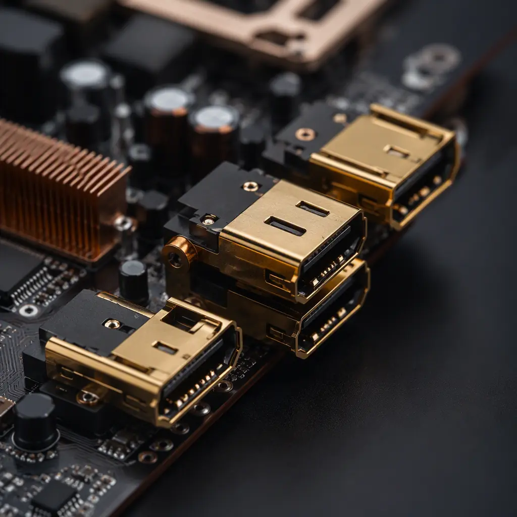
Video interfaces fail on real products for reasons that never show up in the connector datasheet: wrong impedance tolerance in the stackup, vias left un-backdrilled on a 12 Gbps lane, AC coupling caps placed at the wrong end of the pair, or ESD protection with too much capacitance loading the signal. If you are building a monitor, a set-top box, a KVM switch, a medical display, or an automotive infotainment module, the difference between a board that passes HDMI 2.1 compliance and one that flickers at certain resolutions is almost always decided in the PCB layout and the fabrication notes — not in the silicon.
Huaxing PCBA fabricates and assembles high-speed video boards up to 32 layers with controlled impedance at ±5% and TDR verification on every impedance-critical net, under ISO 9001 and IATF 16949. This guide covers the HDMI and DisplayPort routing rules that matter, the stackup decisions behind them, and the exact fabrication requirements to put on your drawing.
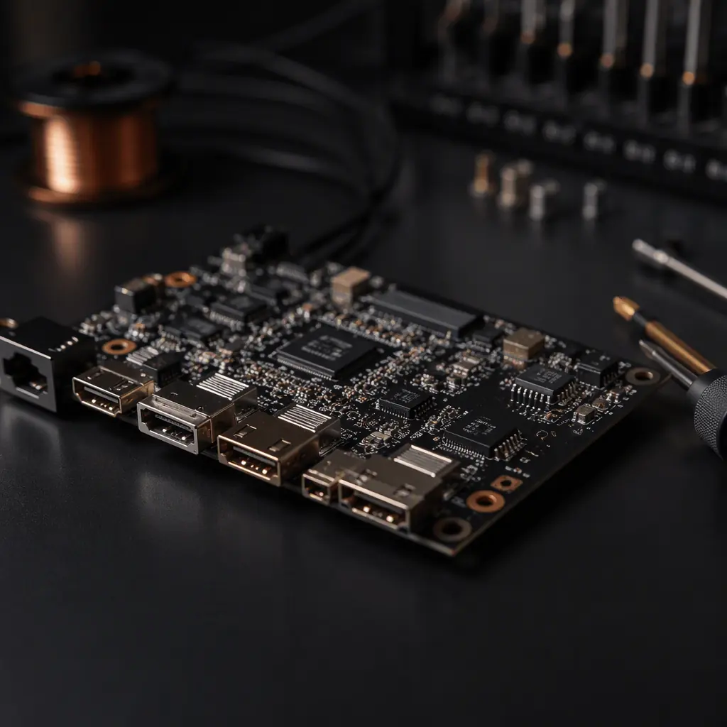
HDMI vs DisplayPort — What the Interface Choice Changes on Your Board
The two interfaces share the same electrical foundation — 100Ω differential pairs with AC coupling — but their data rates and signaling schemes set very different board requirements. Choosing the interface is a product decision; living with its routing rules is a board decision.
| Parameter | HDMI 2.0 | HDMI 2.1 | DisplayPort 1.4 | DisplayPort 2.0 |
|---|---|---|---|---|
| Max bandwidth | 18 Gbps (TMDS) | 48 Gbps (FRL) | 32.4 Gbps (HBR3) | 80 Gbps (UHBR20) |
| Lanes × rate | 4 × 3 Gbps | 4 × 12 Gbps | 4 × 8.1 Gbps | 4 × 20 Gbps |
| Signaling | TMDS | FRL (fixed-rate link) | Main link (8b/10b) | Main link (128b/132b) |
| Differential impedance | 100Ω ±10% | 100Ω ±10% | 100Ω ±10% | 100Ω ±10% |
| AC coupling caps | Optional (source side) | Required on all FRL lanes | Required, 0.1 µF | Required, 0.1 µF |
The practical consequence: a layout that handled HDMI 2.0 at 3 Gbps per lane with moderate care will usually fail HDMI 2.1 FRL at 12 Gbps per lane. At 12–20 Gbps the signal period is under 100 ps, so a via stub of 30 mils, an impedance discontinuity of ±15%, or 200 mils of intra-pair skew is enough to close the eye diagram. If you are designing for HDMI 2.1 or DP 2.0, treat every lane as a high-speed SerDes link, not as a "video trace."
Key Takeaway: HDMI and DisplayPort are both 100Ω differential interfaces, but HDMI 2.1 FRL and DisplayPort 2.0 UHBR require genuine high-speed design discipline — controlled impedance within ±10% (tighter is better), minimal vias, backdrilling or thin dielectrics, and AC coupling caps with controlled placement.
Impedance Targets and Stackup Requirements
Both standards specify 100Ω differential impedance ±10%, measured at the connector reference plane. In practice, compliance testers measure with 25 ps rise-time TDR, so the impedance profile along the entire trace — including the connector launch, the AC coupling cap pads, and the vias — must stay inside the window. A stackup designed for 50Ω single-ended traces does not automatically produce 100Ω differential pairs; the pair geometry (trace width, spacing, and the dielectric height to the reference plane) is a separate calculation.
Choose the Right Layer Count for the Data Rate
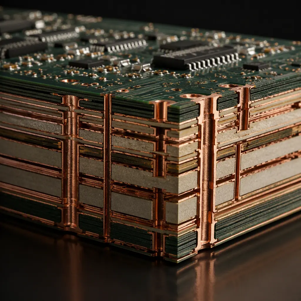
For HDMI 2.0 and DP 1.4, a well-designed 4-layer stackup (signal–ground–power–signal) with the pairs referenced to solid ground planes is workable for short runs under 6 inches. For HDMI 2.1 FRL at 12 Gbps and DP 2.0 UHBR at 20 Gbps, plan 6–8 layers so that every high-speed pair references a solid ground plane on the adjacent layer, power planes are split off, and the connector side can use a low-loss dielectric. Our PCB stackup design guide walks through layer-count trade-offs in detail.
Select a Laminate That Keeps Loss Under Control
Standard FR-4 with a dissipation factor around 0.020 works for HDMI 2.0 at 3 Gbps on short traces. At 12–20 Gbps, dielectric loss and copper roughness dominate: a 10-inch trace on standard FR-4 can lose more than 4–6 dB at 6 GHz, which is roughly the fundamental of a 12 Gbps signal. For FRL and UHBR runs longer than 4–6 inches, specify a mid-loss laminate such as Megtron 6, Isola FR408HR, or Nelco N4000-13 SI family (Df ≈ 0.003–0.005), with smooth or ultra-low-profile copper on the signal layers. Our laminate selection guide compares the material families by loss and cost.
Control Etch Tolerance — It Sets Your Impedance Window
Differential impedance is directly sensitive to trace width and spacing. A standard etch tolerance of ±20% on width can shift a 100Ω pair by 10Ω or more. Specify impedance-controlled pairs with ±10% final tolerance (measured), and let the fab adjust the artwork width to hit the target on your specific stackup — this is standard practice at any capable fab. Ask for ±5% on the pairs that run to compliance-tested connectors. Our impedance control guide explains the measurement and reporting process, including TDR coupons.
Differential Pair Routing Rules for HDMI and DisplayPort
Once the stackup is fixed, the layout rules are mechanical — and measurable. The standards do not specify routing rules directly, but the eye-diagram budgets do, which is why the industry has converged on the following practice.
Match Length Inside the Pair — 5 mils Is the Working Budget
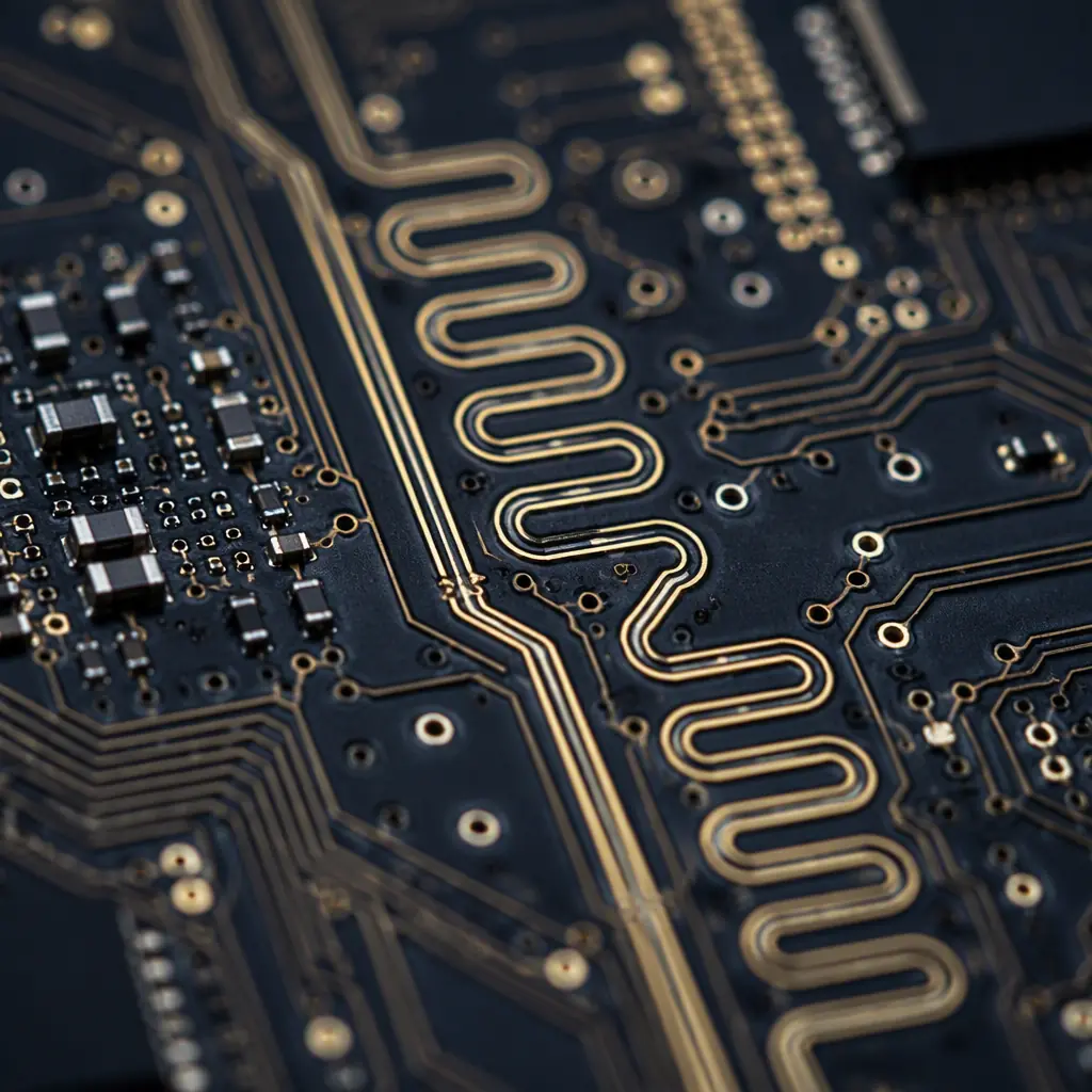
Intra-pair skew of 5 mils (0.127 mm) is the commonly used budget for HDMI 2.0 TMDS and DP HBR3; at FRL 12 Gbps and UHBR 20 Gbps, tighten it to 2–3 mils where the layout allows. Each mil of skew between the P and N lines is roughly 0.17 ps of timing offset at the receiver — small alone, but it adds to jitter from every other source. Use accordion or trombone tuning near the connector end, never in the middle of a tightly coupled run.
Pair-to-Pair Spacing — Give the Lanes Room
Keep at least 3× the dielectric height (usually 20–30 mils) between adjacent differential pairs, and 30+ mils from any aggressor (clock nets, switching regulators). If pairs must run parallel for more than 1 inch, increase spacing to 4×. Crosstalk between adjacent 100Ω pairs at 12 Gbps shows up as deterministic jitter that no equalizer can fully remove. See our crosstalk analysis guide for the math behind the spacing rules.
Vias — Eliminate, Then Minimize, Then Backdrill
Every via on a high-speed pair is a discontinuity: the stub below the signal layer acts as a resonant open stub. At 12 Gbps, a 30-mil stub resonates inside the signal band. Rules of thumb: limit each lane to 2–3 vias; keep via antipad diameter at 2× the drill; and for FRL/UHBR layers below the top surface, specify backdrilling to remove the unused stub. If the design is via-heavy, a thin-dielectric stackup (e.g., 1.6 mm total) can keep stubs short without backdrilling. Our backdrilling guide covers depth control and tolerances.
AC Coupling Caps — Placement and Pad Discipline
DisplayPort requires 0.1 µF AC coupling caps on every main-link lane; HDMI 2.1 FRL requires AC coupling on all four lanes (100 nF–220 nF typical). Place the caps close to the source or connector per the reference design, keep the traces to and from the cap pads symmetric, and use 0402 (or 0201 for UHBR) packages to minimize pad capacitance. The cap pad discontinuity should be tuned with the adjacent trace width — most high-speed reference designs specify a neck-down width for the cap footprint.
Connector Launch — The Most Common Place Eye Diagrams Die
The connector footprint creates the biggest impedance discontinuity on the whole net. Follow the connector vendor's recommended landing pattern exactly, place stitching vias around the connector shield and ground pins (one via per 50–100 mils of shield edge), and avoid routing pairs under the connector body. Route the first 200 mils of each pair away from the connector with constant width and no tuning until the trace is clear of the footprint.
ESD Protection Without Killing the Signal
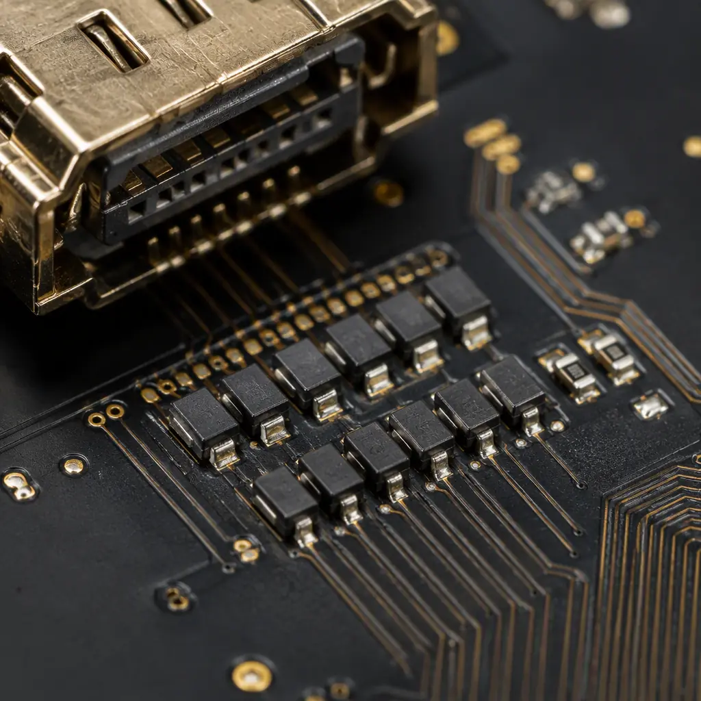
HDMI and DisplayPort connectors are user-accessible, which means they face ESD events of up to ±8 kV contact per IEC 61000-4-2. The tension: a TVS diode with more than 0.5 pF of loading capacitance will round off the edges of a 12–20 Gbps signal even when it is not conducting.
Pick Low-Capacitance TVS Diodes — 0.3 pF or Less
Use TVS devices rated at 0.2–0.5 pF line capacitance per line for HDMI/DP data pairs. Rail-to-rail clamp architectures with integrated diodes are the standard choice; a single 4-channel TVS array covers one differential pair plus its shield. Place the TVS as close to the connector as physically possible — within 100 mils — so the clamp path is short. Our EMC/EMI compliance guide covers the rest of the protection strategy, including filtering and layout for emissions.
Guard the 5V, HPD and DDC/SCL-SDA Lines Too
The +5V and Hot-Plug Detect pins carry no high-speed data and can use standard TVS plus a series resistor. The DDC (I²C) lines for HDMI and the AUX channel for DisplayPort run at 100 kHz–1 MHz — a 1–2 pF TVS is fine there, and series resistors of 22–100Ω help. Skipping protection on these pins is a common field-failure source: an ESD strike on the connector's control pins can corrupt EDID reads or latch the port.
EMI, Shielding and Grounding Around the Connector
Video connectors are also antennas. The TMDS/FRL clocks radiate from the connector body and the exposed pair run, and compliance with FCC Part 15 / CE EN 55032 emissions limits often depends on connector-area design more than on the main board.
Stitch the Shield, Don't Leave It Floating
HDMI connectors ship with a metal shell that must be tied to chassis ground through low-impedance vias. Add stitching vias every 50–100 mils around the connector footprint and connect the shell to the ground plane at both ends. A floating shell turns the connector into a slot antenna. For metal-enclosure products, connect the shell to chassis ground through a 1 nF/2 kV capacitor if the enclosure is separate from the PCB ground.
Keep Switching Power Away From the Video Section
Buck converters and their inductor fields are the most common video noise sources. Place the video interface, connector, and PHY/retimer on one side of the board; keep the switching regulator and its loop at least 300 mils away, on the opposite side of a ground plane. If a regulator must sit near the connector, use a shielded inductor and route the switch node away from the pairs. Our power integrity guide covers plane design for clean power delivery.
What to Write in Your Fabrication Notes
High-speed video boards fail in fabrication review when the requirements are implied rather than stated. Put these five items on the fabrication drawing and the stackup sheet:
Impedance Table With Tolerances
List every impedance net class: 100Ω differential ±10% for HDMI/DP pairs, plus any 90Ω USB or 85Ω PCIe pairs on the same board. Ask for TDR coupons per impedance class on every panel and a TDR report with the shipment. Tolerances tighter than ±10% (e.g., ±5%) are achievable with impedance tuning — state them explicitly if the design needs them.
Backdrilling Requirements
If the design relies on backdrilling, specify the nets (or "all vias on layers X–Y"), the residual stub allowance (typically ≤ 10 mils), and that the backdrill diameter is 8 mils larger than the drill. Confirm the fab's backdrill depth tolerance (±3 mils typical) against your stub budget.
Laminate and Copper Type
Name the laminate family (e.g., Megtron 6, FR408HR) and the copper roughness grade for signal layers. If standard FR-4 is acceptable, say so — but for FRL/UHBR boards, leaving the laminate unspecified invites a cost-driven substitution that loses 3–5 dB at 6 GHz.
Solder Mask on High-Speed Traces
Solder mask over a 100Ω pair changes the effective dielectric and can shift impedance by 2–4Ω. Either design the pair widths for mask-over (the fab's impedance calculator accounts for it) or specify mask removal (NSMD-defined) on the impedance nets. Do not leave it ambiguous.
Connector Assembly Details
Specify whether the connector is hand-soldered or reflowed, the paste stencil thickness for the connector ground pins, and whether a selective solder or press-fit option applies. Connector pins with insufficient solder fillet fail intermittently in the field and are invisible to AOI on the inner rows. Our fine-pitch SMT guide covers stencil and reflow control for dense connector footprints.
Summary: Route for the Standard You Are Shipping, Not the One You Started With
HDMI 2.1 and DisplayPort 2.0 moved video interfaces firmly into the high-speed domain. The board rules are not exotic — 100Ω pairs on solid ground references, controlled etch and impedance, minimal vias with backdrilling, low-capacitance ESD, and disciplined connector launches — but they must be designed in and specified on the drawing, because they cannot be fixed after fabrication. If you are also routing USB-C for DisplayPort Alt Mode, our USB-C design guide covers the shared 100Ω/90Ω routing considerations.
At Huaxing PCBA, we fabricate impedance-controlled boards with ±5% differential targets, TDR-verified coupons, and backdrilling up to 32 layers, and our SMT lines place 0201 components and 0.3 mm-pitch BGA connectors for dense video designs. Read our signal integrity guide for the broader high-speed picture, or send your stackup and impedance requirements to our engineering team for a DFM review with your quote.
