
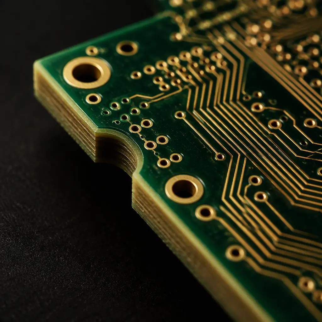
As boards get denser — finer ball pitches, more layers, more signals sharing less area — the through via becomes the bottleneck. It blocks routing channels on layers it does not serve, it eats the breakout space around a BGA, and it adds stub capacitance to high-speed nets. The cure is the via that reaches only the layers it needs to reach. This guide is for the design engineer and the buyer who must decide whether the extra fabrication cost of those vias is justified, and how to specify a high-density interconnect stackup the fabricator can build reliably.
The Three Via Types and What Separates Them
The distinction is mechanical, not electrical. It is about which layers the via's drilled barrel actually reaches.
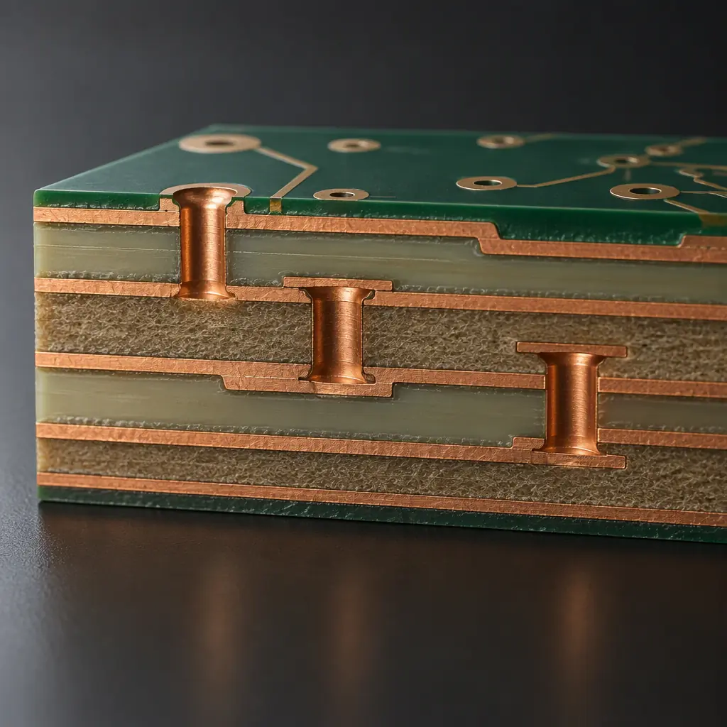
- Through via. Drilled and plated through the entire board stack. Cheapest — one drill cycle, no extra lamination. Occupies every layer.
- Blind via. Reaches an outer layer on one end but stops before the far side. Connects, for example, layer 1 to layer 2 or 3. Requires a controlled-depth drill or laser, and the board must be built so the via can be plated before the outer layers are added.
- Buried via. Reaches only inner layers, with neither end at an outer surface. Connects layer 3 to layer 4, for example. Requires the inner core to be drilled and plated, then laminated into the full stack — that is, a sequential lamination cycle.
The buried via is the more expensive of the two precisely because it is fully internal. A blind via can often be formed by controlled-depth drilling after the board is nearly complete; a buried via must exist on a subassembly that is plated before the board is finished. Every such cycle is a separate lamination press, and each one is a chance for misregistration and yield loss.
Sequential Lamination: Where the Cost Comes From
The cost model of an HDI board is essentially the cost model of how many times it is laminated. A standard through-via board is laminated once. Add a buried via and the board is laminated twice — the inner core is drilled and plated first, then pressed together with the outer layers. A design with multiple buried via levels, or blind vias stacked on buried vias, can need three or four cycles, and the cost does not rise linearly — it rises faster, because each cycle adds a full drill, plate, image and lamination step, and each cycle's yield multiplies against the last.
| Build | Lamination Cycles | Typical Relative Cost | Typical Minimum Drill |
|---|---|---|---|
| Through via only | 1 | 1.0× | 0.20 mm mechanical |
| 1 blind via level (1–2) | 1–2 | 1.4–1.8× | 0.10 mm laser |
| 1 buried via level | 2 | 1.6–2.0× | 0.15 mm mechanical |
| Blind + buried (stacked) | 3 | 2.5–3.5× | 0.10 mm laser |
| Any-layer / ELIC | 4+ | 4×+ | 0.075 mm laser |
The numbers are indicative — actual cost depends on layer count, via density, panel utilisation and quantity — but the shape of the curve is what matters. Before specifying buried vias, confirm that routing density genuinely cannot be solved a cheaper way, because the cost step between one and three lamination cycles is large and permanent.
The Cheaper Alternatives to Reach For First
Buried and blind vias are the last tool in the box, not the first. Before committing to extra lamination, work through the cheaper options that solve the same routing-density problem:
- More layers with through vias. If board thickness allows, adding a layer pair and using through vias is almost always cheaper than adding a lamination cycle.
- Backdrilling. For high-speed nets where the problem is via stub rather than density, backdrilling the unused via barrel removes the stub without adding lamination — a targeted fix that costs far less than buried vias. The reliability implications are covered in the via reliability comparison.
- Via-in-pad with fill and cap. Where the problem is breakout space under a fine-pitch BGA, filled and capped via-in-pad frees the pad for placement without a buried via. See the filled via and via-in-pad guide for the process requirements.
- Dog-bone fanout with a shallower BGA escape. Sometimes the density problem is really a fanout strategy problem, solved by routing rather than by via type.
Only when each of those has been ruled out — and the density or stub requirement truly cannot be met — is the sequential-lamination cost worth paying. Reaching for buried vias first is one of the most common and most expensive over-specifications in PCB design.

Aspect Ratio, Registration and the Design Rules That Decide Buildability
Once buried or blind vias are chosen, three physical rules determine whether the board can be built at a reasonable yield:
- Aspect ratio. The ratio of via depth to drilled diameter governs how reliably the barrel can be plated. For mechanical drills, an aspect ratio above about 10:1 becomes difficult; laser-drilled microvias in thin dielectric are held far lower, typically under 1:1 because the dielectric is only 50–100 µm thick. Specify via diameters that keep the ratio inside the fabricator's proven window.
- Registration tolerance. Every lamination cycle introduces layer-to-layer registration error, and blind and buried vias must land on their target pads despite it. Allow generous annular rings — often 0.10–0.15 mm minimum for inner-layer targets — because a misregistered via that breaks out of its pad is a reliability defect, not just a routing one.
- Stacked vs staggered vias. Stacking a microvia directly on top of a buried via concentrates mechanical stress and demands very tight registration. Staggering (offsetting) them is more reliable and cheaper; only use stacked vias where density leaves no alternative, and expect the fabricator to require tighter process control.
These constraints are the reason an HDI stackup must be designed together with the fabricator, not handed over as finished artwork. The stackup design guide covers the broader layer-assignment decisions that these via rules feed into, and the via aspect ratio guide goes deeper on the plating limits.
Specifying the Stackup on the Drawing
An HDI stackup drawing should state, at minimum: the layer count and the signal/plane assignment; for each via type, which layers it connects (expressed as a span, for example 1–2 or 3–4); the finished via diameter and pad (annular ring) for each; the lamination sequence as an ordered list of cycles; and the controlled-depth or laser-drill requirement for blind vias. Ambiguity here is the single biggest cause of an HDI board coming back unbuildable, because the fabricator has to guess the intent and the guess is usually the cheapest interpretation, which is wrong.
At Huaxing PCBA, HDI builds up to 32 layers with blind, buried and stacked-microvia stackups are quoted from a released stackup drawing, with the lamination sequence and registration tolerances confirmed at DFM before any material is cut. We build to IPC-6012 Class 2 and 3 and run IST and thermal-shock via reliability testing on qualification lots. Send your stackup drawing and Gerber for an HDI quote or talk to an engineer about your stackup before you commit to a lamination sequence.
