
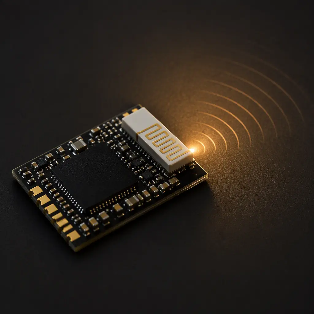
Ultra-wideband has become the precision ranging standard of the IoT world: phone-as-car-key systems, industrial asset trackers, smart-home presence detection, and hands-free access control all use UWB because it measures distance with ±10 cm accuracy — roughly 20-50 times better than Bluetooth RSSI ranging. Instead of measuring received signal strength, a UWB radio transmits sub-2 ns impulse pulses across a 499.2 MHz channel and measures time-of-flight directly. The market moved fast: UWB shipments passed 500 million units in 2024 and automotive digital keys are now fitted to most new EV and premium ICE platforms.
Huaxing PCBA manufactures UWB modules and digital-key ECUs for automotive, IoT, and industrial customers — 2-32 layer stackups with 3/3 mil capability, laser microvias for compact RF modules, impedance control to ±5%, and 8 SMT lines with X-ray and RF functional test support. This guide covers the RF front-end layout, antenna and phase-center rules, BLE coexistence, automotive requirements, certification, and the DFM specifications you should put on the fabrication drawing.
Why UWB Layout Is Different From Any Other Radio
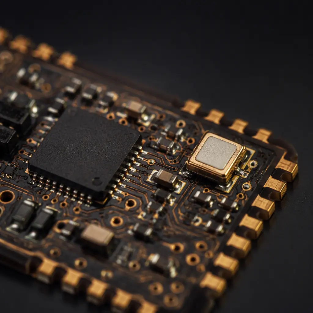
Most RF boards are designed for a single carrier frequency. UWB is a time-domain technology: the receiver digitizes a wideband pulse and measures when it arrives. That changes what matters on the PCB in three specific ways.
The Bandwidth Spans 3.1-10.6 GHz, Not a Single Carrier
FiRa Consortium devices operate on Channel 5 (6.4896 GHz) or Channel 9 (7.9872 GHz), each with a 499.2 MHz channel bandwidth. A matching network tuned for one frequency is useless here — every reactive element must stay flat across the whole 500 MHz channel, or the pulse shape distorts and the leading-edge timing that ranging depends on shifts. Keep the RF path short, use components rated well above 8 GHz, and avoid high-Q resonances near the passband.
Group Delay Variation Becomes a Ranging Error
A 1 ns timing error is a 30 cm distance error, because the radio pulse travels at roughly 0.3 m/ns. Group delay variation across the channel — from a poorly grounded via fence, a mismatched trace, or an out-of-band filter resonance — directly corrupts the time-of-arrival measurement. UWB receivers calibrate out fixed delays, but frequency-dependent delay variation cannot be calibrated. The practical rule: one clean, short, controlled-impedance path from the transceiver to the antenna, with no stubs, no layer changes, and no unnecessary filtering in the RF line.
Antenna Phase Center Is Part of the Measurement
Ranging accuracy depends on where the antenna appears to radiate from — its phase center — not where the component is physically placed. A chip antenna with a datasheet-specified ground clearance, mounted exactly as recommended, has a stable phase center; a trace antenna bent to fit a crowded board corner does not. For automotive digital keys the antenna position on the vehicle must also be reproducible across production, so the design rules for antenna placement are stricter than for a BLE tag.
Key Takeaway: UWB is a time-domain radio. Anything that varies with frequency — group delay, matching ripple, antenna detuning — becomes a ranging error. The RF path must be short, flat, and predictable, not just low-loss.
The RF Front End: Transceiver, Matching, and Grounding
UWB designs are built around a single-chip transceiver — Qorvo DW3110/DW3120, NXP SR150/SR040, or NXP NCJ29D5 for automotive — usually paired with a companion MCU. Our IoT PCB design guide covers the system architecture these radios sit inside; here are the RF-specific rules.
Copy the Reference Design's RF Section Verbatim
The transceiver datasheet specifies the balun, matching components, and antenna-port layout for each channel. Use the exact component values and footprint placements from the reference design — do not relocate the matching network "for convenience." The differential RF pins need their ground pins connected to a continuous ground pour directly beneath the IC, with vias at every ground pad. A stray 1-2 nH of via inductance here detunes the match across the wide channel.
Route the 50 Ω Feed as a Tight, Continuous Line
From the matching network to the antenna or connector, keep a controlled 50 Ω line — microstrip or grounded coplanar waveguide — on one layer, with no vias in the RF path. On a typical 1.6 mm FR-4 stackup, a CPWG trace around 1.0-1.2 mm wide with 0.3 mm gaps to ground pours on both sides works for the UWB band; verify the exact geometry against your stackup with the fab's impedance calculator. Add ground stitching vias beside the line every 2-3 mm. Specify ±10% impedance control and verify with TDR — our impedance control guide explains the coupon requirements.
Isolate the RF Section With a Grounded Via Fence
UWB receivers digitize pulses at GHz sample rates, and the digital switching noise from the companion MCU can couple straight into the antenna port. Surround the RF section with a via fence (vias on ~0.5 mm pitch) connecting all ground pours, keep the antenna and RF trace away from the MCU's clock and SPI lines, and never route digital signals on the layer directly beneath the antenna. If the board uses a shield can, ground its mounting pads with multiple vias to the main plane.
Key Takeaway: The RF chain is: transceiver → balun/matching → 50 Ω feed → antenna. Every transition must be tight, grounded, and impedance-controlled — and the wide channel bandwidth leaves no room for resonances that a narrowband design would tolerate.
Antenna Selection and Phase-Center Rules
UWB antenna choice trades size, cost, and angular coverage against ranging reliability. Our PCB antenna design guide covers antenna fundamentals; the UWB-specific considerations are below.
| Antenna Type | Typical Size | Pattern | Best For |
|---|---|---|---|
| Ceramic chip antenna | 3-8 mm × 1-2 mm | Omnidirectional, needs ground clearance | Tags, trackers, compact modules |
| PCB monopole / dipole | 12-25 mm element | Omnidirectional in one plane | High-volume, low BOM cost |
| Printed monopole + ground plane | 20-40 mm total | Quasi-omnidirectional | Industrial tags, anchors |
| External/UWB-rated antenna | Connector + antenna | Wideband, stable phase center | Anchors, automotive ECUs, fixed infrastructure |
Follow the Chip Antenna's Clearance Drawing Exactly
Chip antenna datasheets specify a ground clearance zone, a recommended board-edge location, and often a matching network. Ignoring the clearance — placing the antenna over a ground pour, or a trace crossing the keep-out area on an inner layer — can cost 5-8 dB and shift the phase center. Copy the manufacturer's recommended layout including any ground cutout, and keep the antenna area clear of solder mask per the datasheet.
For Automotive Digital Keys, Plan Antenna Placement Per Vehicle Zone
Car makers place 4-8 UWB anchors around the vehicle (door handles, trunk, center console) so the phone's position can be triangulated. Each anchor PCB needs its antenna oriented for the coverage zone, with a stable phase center and a mounting position that is repeatable in production. This is a mechanical and layout planning task as much as an RF one — specify the antenna location and orientation on the assembly drawing, and use fixtures in production to hold it.
Test the Antenna in the Final Enclosure
UWB performance changes with nearby metal, battery packs, and enclosures — a tag inside a metal-backed asset tracker can lose most of its range. Always characterize return loss and pattern with the final housing and battery present. If the enclosure is plastic with conductive coatings, verify the antenna still radiates before committing to tooling. Our RF PCB manufacturing guide covers the fabrication side of antenna- and impedance-critical boards.
BLE Coexistence: The Dual-Radio Design Problem
Most UWB products also carry BLE — the phone digital-key ecosystem uses BLE for wake-up and handshake, then UWB for precise ranging. Putting two radios on one board creates a classic coexistence problem.
Keep the Two Antennas at Opposite Edges
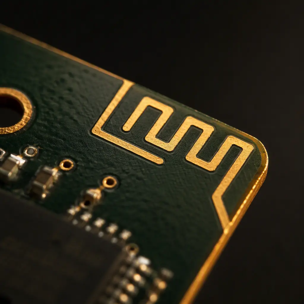
The BLE antenna (2.4 GHz) and the UWB antenna (6.5-8 GHz) should sit at opposite corners or edges of the board, with their keep-out zones non-overlapping. This is not just about detuning — it minimizes coupling of the BLE transmitter's harmonics and the UWB pulses into each other's receivers. A minimum separation of 20-30 mm is a practical target for compact modules. Our BLE PCB design guide covers the 2.4 GHz side of the layout.
Coordinate Power and Clock Domains
Both radios share the same supply rails and often the same crystal or reference clock. Use separate LDO/DC-DC outputs for the RF sections with individual ferrite-bead filters, and keep the UWB crystal and its load capacitors close to the transceiver. If a single crystal drives both radios, follow the reference design's buffer arrangement exactly — a shared-clock layout error is a classic source of intermittent ranging failures. See our power integrity guide for supply filtering detail.
Design the Antenna Switch and T/R Path for Both Bands
Time-division products switch between TX and RX on the UWB path (or between BLE and UWB on a shared antenna). The switch's isolation, insertion loss, and return loss must hold across both bands. Use parts rated for the full 3.1-10.6 GHz range even if you only use Channel 5/9 today — it keeps the design reusable and avoids a respin when a customer asks for the other channel.

Automotive Digital Key: Requirements Beyond the Radio
Phone-as-car-key is the highest-volume UWB application, and it pulls in requirements that a consumer tag never sees. Our automotive PCB requirements guide covers the platform-level rules; the UWB-specific ones follow.
Automotive-Grade Parts and Process From Day One
UWB anchor ECUs live in door handles and bumpers: operating temperature from -40°C to +105°C, vibration per ISO 16750, and AEC-Q100-qualified components. The fabrication must be IATF 16949-certified with PPAP documentation, IPC-A-610 Class 3 assembly, and full lot traceability. Huaxing holds IATF 16949 and runs automotive production with X-ray inspection and 100% functional test on UWB anchors.
Security and Ranging Integrity Are Board-Level Concerns
UWB digital keys rely on time-of-flight to stop relay attacks — a relay amplifier that tricks a BLE-only car key is defeated because the UWB time-of-flight measurement reveals the extra distance. The PCB supports this by keeping the antenna phase center stable and the RF path clean so measured delays are deterministic. Physical tamper protection on the anchor (secure MCU, tamper mesh options) is specified at the system level, but the board layout must keep security-critical traces away from board edges where they can be probed.
Plan the RF Test Coverage Per Anchor
Every anchor needs a production RF test — transmit power, pulse shape, and frequency — plus an antenna check in the final housing. Add test points on the RF feed and a test mode in firmware. Our PCB testing methods guide shows where RF functional test fits in the overall test strategy, alongside AOI, X-ray, and flying-probe.
Certification: FCC Part 15.517/15.519 and Beyond
UWB is regulated differently from narrowband radios because it operates under a power spectral density limit rather than a total power limit.
Know the Emission Limit That Drives the Design
In the US, indoor UWB systems fall under FCC Part 15.517 and handheld devices under 15.519, both capped at -41.3 dBm/MHz EIRP. Europe uses ETSI EN 302 065 (with the same -41.3 dBm/MHz low-duty-cycle limit for many use cases). The wide 500 MHz channel spreads the energy so thin that meeting the limit is usually about controlling out-of-channel emissions — harmonics of the 499.2 MHz channel spacing, clock spurs, and switching noise from the digital section — rather than the main pulse. A clean layout and a shielded RF section are the cheapest insurance. See our EMI/EMC design guide for the general emissions-control playbook.
Use a Certified Module to Shorten Time-to-Market
Pre-certified UWB modules (FCC/CE approved) dramatically cut the certification path for tags and anchors — the radio portion is largely covered, and the end product mainly needs enclosure and system-level testing. If you integrate the bare transceiver, budget for conducted and radiated pre-compliance testing before the full run. Either way, keep an RF test point in the feed so the lab can measure without modifying the board.
Document the Antenna Configuration for the Filing
UWB certifications are filed for a specific antenna configuration. If you swap the antenna type after certification, the filing may not cover the new configuration. Lock the antenna BOM and the board revision that passed testing, and keep the test report with the production documentation. FiRa certification (for interoperability) is a separate program that buyers increasingly request for tags and anchors — plan for it if your product targets the phone ecosystem.
DFM for UWB Boards: What to Put on the Drawing
A UWB board is usually a compact 4-8 layer HDI design, and the RF section imposes requirements a standard digital fab drawing may not cover. Specify these explicitly:
Impedance Control With Per-Panel Coupons
Request ±10% impedance control on the 50 Ω RF feed (tighter if your simulation says so), with coupons on every panel and reported measurement data. The coupon must mirror the real stackup — same dielectric, same trace geometry. Do not accept "impedance verified" without numbers. Our stackup design guide covers defining this correctly.
Controlled Dielectric and Microvia Tolerances
The RF feed impedance depends on the laminate's dielectric constant. Specify FR-4 with a known Dk (4.2-4.5) or a controlled-Dk laminate for the RF layer, and fix the copper weight. Compact UWB modules use laser microvias (0.075 mm, which Huaxing supports) for fan-out under the transceiver — note the via-in-pad and filling requirements for any pad under the IC. Our HDI technology guide explains the microvia stackup options.
Keep the Antenna Area Free of Mask, Silkscreen, and Copper
Specify solder mask removal over the antenna element, keep silkscreen and component identifiers out of the keep-out zone, and confirm no copper pour or trace crosses the clearance area on any layer. If the antenna connects via a castellation or edge plating, note the plating requirements — edge-plated castellations are routine for module-style UWB boards. Our solder mask guide explains mask options.

Summary: The UWB Board Checklist
A UWB product that delivers centimeter-level ranging is designed with a short, flat RF path from transceiver to antenna, a grounded via-fenced RF section, an antenna with a stable phase center and datasheet-exact clearance, BLE and UWB antennas isolated at opposite edges, a power tree that keeps switching noise off the RF rails, and a fabrication drawing that specifies impedance coupons, controlled dielectric, microvia tolerances, and mask-free antenna areas. On the production side, RF functional test on every unit — transmit power, pulse shape, and frequency — catches the defects that field ranging failures would otherwise reveal months later.
At Huaxing PCBA we manufacture UWB modules and automotive anchors up to 32 layers with laser microvias, controlled-impedance capability to ±5%, mixed FR-4 and high-frequency laminates, and full RF assembly support — 8 SMT lines, X-ray for shield cans and BGA, and flying-probe plus RF functional testing. Our DFM review checks the RF stackup, impedance coupons, antenna keep-outs, and assembly requirements before tooling. Read our GNSS receiver design guide for the other precision-positioning radio, or send your files for a free DFM review and quote.
