

When a shipment of assembled boards arrives, the question that decides whether you accept or reject it is: does this workmanship meet the acceptance criteria in the contract? For the vast majority of electronics buyers, that criteria document is IPC-A-610 — the most widely used assembly acceptance standard in the world, referenced in 3,000+ corporate and military procurement specifications. It defines, with photographs and measurement tolerances, what a good solder joint looks like, how much component damage is tolerable, and what level of cleanliness is acceptable. Without it, "defective" is an opinion; with it, "defective" is a measurement.
At Huaxing PCBA, we assemble boards to IPC-A-610 Class 2 and Class 3 on 8 SMT lines, with certified IPC-A-610 trainers performing final inspection on every lot. This guide walks you through the criteria that actually matter when you open the box — the solder joint rules, the damage limits, the contamination thresholds — plus the checklist we recommend you run at incoming inspection. If you are new to the standard family, our IPC standards comparison guide explains how A-610 fits with IPC-A-600, J-STD-001, and IPC-6012.

What IPC-A-610 Actually Governs — and What It Doesn't
IPC-A-610 is an acceptance criteria document for assembled electronic products. It answers one question: given a board that is already assembled, is the workmanship acceptable? It is deliberately visual — it uses photographs and illustrations of target, acceptable, and nonconforming conditions rather than process instructions. That is what makes it the default reference in purchase orders: a buyer and a supplier can both look at the same joint and agree on the verdict.
| Standard | Governs | Typical Use in a PO |
|---|---|---|
| IPC-A-610 | Acceptance criteria for assembled boards — solder joints, component damage, cleanliness, marking | "Assemble to IPC-A-610 Rev H, Class 2" |
| IPC-A-600 | Acceptance criteria for bare printed boards — laminate, plating, registration | "Fabricate to IPC-A-600 Class 3" |
| J-STD-001 | Process requirements — materials, soldering methods, verification | "Process per J-STD-001, Class 3" |
| IPC-6012 | Qualification/performance of bare boards — electrical, mechanical, environmental | "Qualify per IPC-6012 Class 3" |
Two practical consequences follow. First, A-610 is not a process standard — it does not tell the assembler how to solder, so it is normally paired with J-STD-001 in the same contract. Second, A-610 says nothing about the bare board itself; laminate defects, plating voids, and registration errors are judged against IPC-A-600 and IPC-6012, which we cover in our IPC-A-600 acceptance guide. When your incoming inspection flags a defect, the first step is always to identify which standard applies to that defect class.
Class 1, 2, and 3: How Acceptance Stringency Scales
IPC-A-610 defines three product classes, and the class in your contract determines the acceptance limits for every single criterion in the document:
Class 1 — General Electronic Products
Consumer products where the primary requirement is function of the completed assembly. Acceptance limits are the most lenient: cosmetic imperfections that do not affect function are acceptable. Examples: disposable consumer electronics, toys, basic lighting.
Class 2 — Dedicated Service Electronic Products
Products where extended life and uninterrupted service are required, but failure is not life-critical. This is the default class for most industrial, telecom, and commercial equipment. Cosmetic imperfections are acceptable if they do not affect reliability. Most commercial EMS work ships Class 2.
Class 3 — High-Performance / Harsh Environment Electronic Products
Products where continued performance is critical — failure cannot be tolerated (life support, avionics, military, automotive safety). The most stringent acceptance limits in the document: no cosmetic imperfections permitted that could affect reliability, tighter fillet and damage tolerances, and 100% inspection of many criteria. Expect Class 3 to add 15-30% to assembly and inspection cost versus Class 2, driven by stricter criteria and denser inspection coverage. Our IPC Class 2 vs Class 3 guide breaks down where that cost actually goes.
The class must be written into your contract before production — you cannot "upgrade" a shipment to Class 3 after it is built, because the inspection coverage was planned around the contracted class. And note that A-610's class definitions apply to the end product: a board that goes into a Class 3 medical pump must be inspected as Class 3 even if the bare board was fabricated to a lower class.

The 5 Solder Joint Criteria That Decide Accept or Reject
Most incoming-inspection disagreements are about solder joints. IPC-A-610 evaluates every joint — through-hole, chip component, gull wing, BGA — against a small set of measurable criteria. These are the five that generate the most disputes between buyers and assemblers:
Wetting Angle: The Joint Must "Wet" the Surfaces
The solder must wet both the lead/termination and the pad, forming a contact angle of ≤ 90° between the solder and the surface. An angle greater than 90° indicates poor wetting (dewetting), which is a reject condition for all classes. This is the fastest single check a buyer can make under a microscope: glossy, concave fillets = good wetting; dull, convex, balled solder = dewetting.
Minimum Fillet Height: Solder Thickness + 25% of the Lead
For through-hole joints, the solder fillet must extend up the lead to a minimum height of solder thickness + 25% of the lead diameter (Class 2 and 3). For chip components, the minimum fillet height is solder thickness + 25% of the termination height. A fillet that stops below this line does not guarantee a reliable mechanical and electrical connection and is rejectable.
Side Fillet Length on Chip Components: 75% of the Termination
On chip components (0402, 0201, 01005), the solder must wet along at least 75% of the termination length (Class 2), measured on the side fillet. Class 3 raises related requirements on fillet height and adds requirements for the solder to visibly wet the end cap. This is why tiny passives are the most common source of A-610 rejects — their small terminations leave little room for fillet variation. See our fine-pitch SMT assembly guide for how placement and stencil design keep these fillets in spec.
Voiding in BGA and QFN Joints: X-Ray Is the Only Way to See It
For area-array components, A-610 defers void evaluation to X-ray. The widely applied guidance (IPC-7095) caps void area at 25% of the ball cross-section for Class 2 and 15% for Class 3, with tighter limits on voids clustered under thermal pads. This criterion cannot be checked visually — your incoming inspection must include X-ray sampling for BGA/QFN products, or you are accepting blind. Our AOI / X-Ray / SPI inspection guide covers the equipment and sampling rates.
Component Damage: Cracks Never, Chipping Within Limits
Cracks in the component body are a reject at any class. Chipping is allowed only within measured limits: for ceramic chip components, chipping must not expose the internal metallization, and total edge damage is limited to 25% of the chip's width (Class 2) with tighter limits for Class 3. Damaged components from handling, rework, or depaneling are the second most common reject category — which is why our depaneling guide emphasizes method selection as a yield issue, not just a throughput one.
Contamination and Cleanliness: The Criterion Most Buyers Forget
Solder joints are visible; ionic contamination is not — but it causes corrosion, dendrite growth, and field failures months after acceptance. IPC-A-610 requires that assembled boards be free of flux residues, oils, and other contaminants that could affect reliability. The measurable enforcement is J-STD-001's ionic cleanliness limit of ≤ 1.56 μg/cm² NaCl equivalent (for rosin-based processes requiring cleaning), verified by ROSE or ion chromatography; for no-clean processes, acceptability is judged by the A-610 visual criteria combined with surface insulation resistance (SIR) testing per IPC-9202. If your product is high-humidity or high-voltage, specify the cleanliness test explicitly in the PO — do not assume the assembler runs ROSE by default. Our ionic contamination testing guide explains the methods and limits in detail.
Key Takeaway: The most expensive acceptance mistake is inspecting only solder joints. A board can pass every visual criterion and still fail in the field from contamination, hidden voids, or internal component damage. For Class 2/3 products, pair visual inspection with X-ray sampling and an ionic cleanliness test at first article — 3 checks that together cover what the eye alone cannot see.
How to Write IPC-A-610 Into Your Purchase Order
Acceptance criteria are only enforceable if they are in the contract. We recommend four clauses on every assembly PO:
Standard + Revision + Class, Explicitly
Write "IPC-A-610 Rev H, Class 2" (or 3) — not "IPC-A-610" alone. Revisions change criteria; without a revision pin, a dispute can hinge on which edition applies. Also state the governing class of the end product, since A-610 classes describe the product, not the factory.
Deviations in Writing
Any relaxation or tightening (e.g., "X-ray void limit 20% for the thermal pad") must be a written deviation attached to the PO. Verbal allowances are unenforceable and are the #1 source of post-shipment disputes.
Inspection Data Deliverables
Require the assembler to ship the inspection records: AOI/SPI logs, X-ray reports for area-array lots, first article inspection (FAI) results, and — if specified — ionic cleanliness reports. Our FAI guide lists the documents a complete first-article package contains.
Disposition Process for Nonconforming Lots
Agree in advance on the path for rejects: 8D corrective action, sort/repair vs. scrap decision rights, return freight responsibility, and the deadline for replacement. A written disposition clause turns a quality dispute into an administrative step. Our quality dispute resolution guide covers the common clause structures.
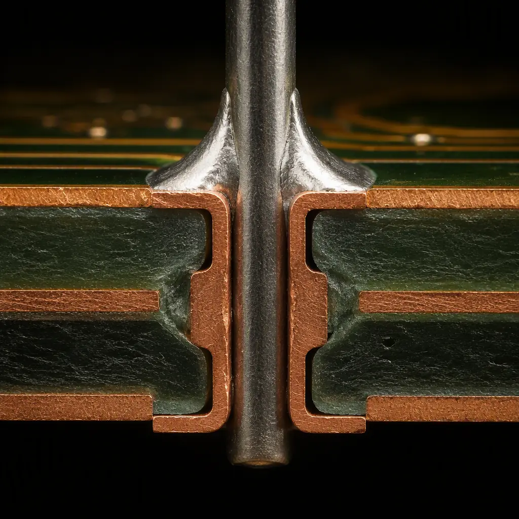
A Buyer's 15-Point Incoming Inspection Checklist
Use this checklist when you receive assemblies. It is written to be executable by a trained inspector with a microscope, X-ray access (for area-array products), and a copy of the contracted revision:
Documentation
Certificate of conformance (CoC) states the standard, revision, class, and lot/date codes; packing list matches PO quantities.
Sampling Plan
Sample size defined in advance (e.g., ANSI/ASQ Z1.4 General Level II, AQL 1.0 for visual, 0.65 for functional) — documented before inspection, not after.
Solder Joint Wetting
Spot-check wetting angle ≤ 90° on a sample of through-hole and chip joints across board quadrants.
Fillet Height
Verify minimum fillet height (solder thickness + 25% of lead/termination dimension) on through-hole and chip components.
Chip Side Fillet
Side fillet covers ≥ 75% of termination length on chip passives (Class 2).
BGA/QFN Voids
X-ray sample: void area within the contracted limit (25% Class 2 / 15% Class 3 per IPC-7095 guidance).
Component Damage
No cracks; chipping within width limits and not exposing metallization.
Misalignment
Component offset within A-610 limits (chip offset ≤ 25% of pad width for Class 2/3; no tombstoning, no skew beyond fillet coverage).
Polarity and Marking
All polarized components (diodes, electrolytics, ICs) correctly oriented; reference designators legible.
Cleanliness
No visible flux residue around joints (per A-610 visual limits for the flux type); ROSE report if contracted.
Conformal Coating
If coated: coverage, no bubbles/delamination, no coating on test points/connectors — per the coating criteria in A-610. See our conformal coating guide.
Mechanical Assembly
Connectors seated, fasteners torqued, no foreign object debris (FOD) inside the enclosure.
Electrical Test Evidence
ICT/flying probe or functional test reports included, pass rates within contract. See our testing methods guide for what each report should contain.
Traceability
Lot/date codes marked and mapped to build records — required for any product with a recall or warranty path. Our IPC-1782 traceability guide covers the data standards.
Packaging and Handling Evidence
ESD-safe packaging per the agreed standard, moisture-barrier bags with intact humidity indicator cards for MSL components, and no physical damage in transit. Our ESD packaging standards guide lists the box-level checks.
Run this checklist on first article before production, then on a contracted sampling basis per lot. For a deeper look at how to structure the incoming inspection agreement itself — sample sizes, AQLs, and hold/release authority — our incoming quality inspection guide and quality metrics guide give the benchmarks your assembler should be reporting against.
How Huaxing PCBA Implements IPC-A-610
IPC-A-610 is not a poster on our wall — it is the operating system of our quality department. Every Huaxing assembly order ships with a CoC stating the contracted standard, revision, and class. Our SMT lines run 100% AOI with 3D SPI on every printed panel, X-ray sampling on all area-array lots, and final inspection performed by IPC-A-610 certified inspectors. First articles are documented against the contracted class, and customers receive the inspection records with the shipment. If you are specifying a new product, send us your Gerber, BOM, and your class requirement — our engineers will confirm the acceptance plan, the inspection coverage, and the criteria that apply to your specific component mix before production starts, and return a quote with the full acceptance criteria mapped to your contract.
Send your assembly files and class requirement to our quality team for a 24-hour quote with the IPC-A-610 acceptance plan included.
