
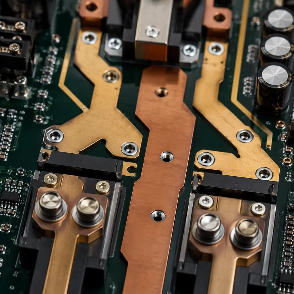
The global new energy PCB market is projected to exceed $12 billion by 2028, driven by EV infrastructure buildout, grid-scale battery storage, and solar deployment. But procurement teams entering this space quickly discover that specifying PCBs for new energy products is fundamentally different from ordering boards for consumer electronics or even standard industrial equipment.
A PCB inside an EV fast charger handles 500A at 800V while sitting in an unventilated outdoor enclosure in Arizona. A battery management system board runs 32 layers of precision analog sensing next to 6oz copper power planes on a Rogers substrate. A solar inverter PCB must survive 15 years of daily thermal cycling from -20°C to +85°C without delamination. These are not edge cases, they are baseline requirements. At Huaxing PCBA, our Shenzhen facility handles new energy PCB production with 6oz copper capability, 32-layer stackups, and IATF 16949 certified processes serving 150+ customers across 30+ countries.
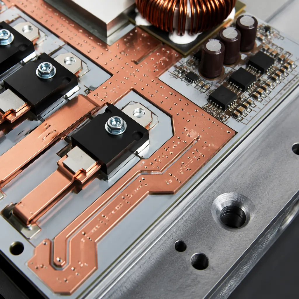
Why New Energy PCBs Are Different from Standard Industrial Boards
The gap between a standard industrial control PCB and a new energy-grade board comes down to four stress vectors that operate simultaneously:
| Stress Factor | Standard Industrial | New Energy Requirement |
|---|---|---|
| Current density | 1-2oz Cu, ~35A max | 4-6oz Cu, 200-500A continuous |
| Voltage isolation | 500V-1kV | 1.5kV-4kV (EV charger safety isolation) |
| Thermal cycling range | -10°C to +70°C | -40°C to +125°C (automotive-grade) |
| Lifetime expectancy | 5-8 years | 15-25 years (solar inverter field life) |
| Environmental exposure | Indoor, controlled | Outdoor, IP65 enclosure, UV, humidity, salt spray |
| CTI requirement | PLC 3 (175-249V) | PLC 0-1 (≥400-600V) for creepage |
Each of these factors cascades into substrate material selection. Standard FR-4 hits its glass transition temperature (Tg) at 130-140°C. In an EV charger, internal ambient temperatures routinely exceed 100°C during peak load. The margin is too thin. New energy designs demand High-Tg FR-4 (Tg170-180), polyimide for flex sections, or ceramic-filled hydrocarbon substrates (Rogers 4350B, Megtron 6) for RF power sections. The material cost is 3-8× higher. And the consequences of choosing wrong are field failures measured in millions of dollars in warranty claims.
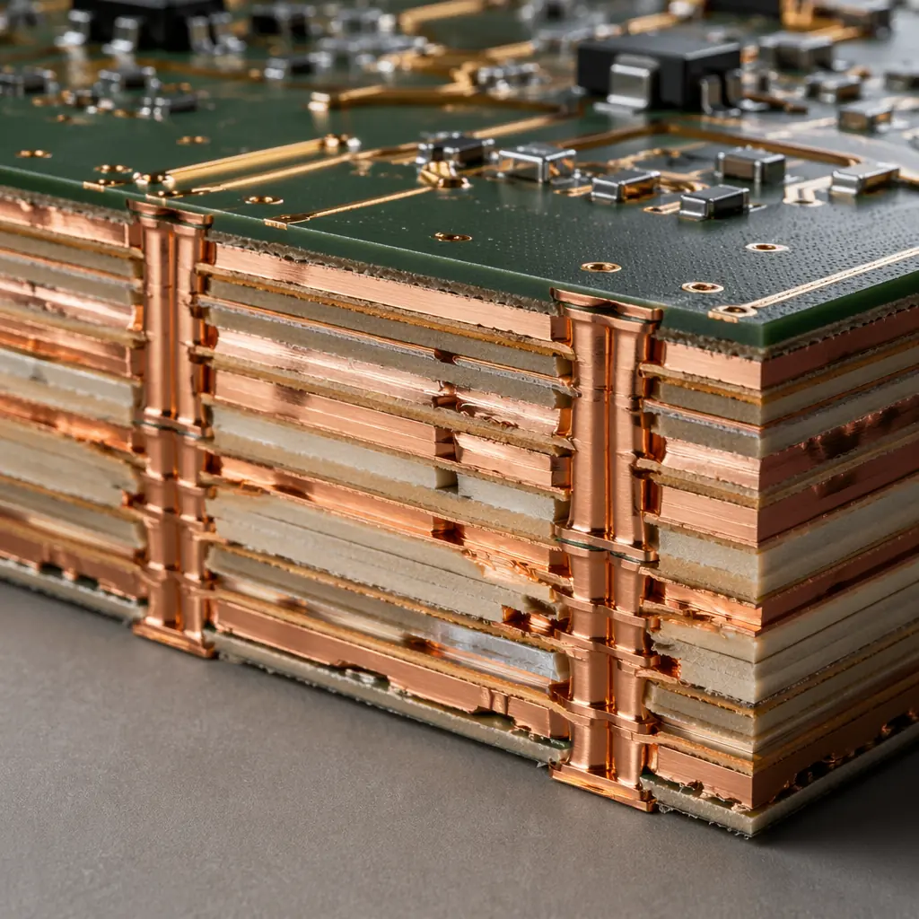
EV Charging Station PCBs, High Power, Thermal Cycling, Outdoor Reliability
An EV DC fast charger delivers 50-350kW through power electronics that operate at switching frequencies of 20-100kHz. The PCB inside the power module handles three things simultaneously: high-frequency switching with minimal EMI, high-current routing with acceptable I²R losses, and thermal dissipation that keeps junction temperatures below 150°C.
Critical PCB specs for EV charger power modules
- Copper weight: 4-6oz on power planes. Below 4oz, trace width becomes impractical for 200A+ paths. At 6oz, a 50mm-wide trace handles ~300A with a 20°C rise, feasible on a 600×800mm panel.
- Thermal management: Metal-core PCBs (aluminum or copper base) for direct-bonded IGBT/SiC modules. Thermal conductivity of 2-8 W/m·K vs 0.3 W/m·K for standard FR-4.
- Creepage and clearance: IEC 61851-23 requires 4mm creepage for 800V systems at pollution degree 2. This constrains component placement and requires slot routing between high-voltage and low-voltage domains.
- Partial discharge resistance: Voltage transients during switching can initiate partial discharge in voids within the PCB laminate. High-Tg materials with controlled impedance and void-free lamination are non-negotiable.
- Conformal coating: Outdoor chargers need acrylic or silicone conformal coating (IPC-CC-830) to prevent moisture-induced leakage currents across exposed copper between conformal coating and solder mask edges.
Production reality: We manufacture EV charger power boards at 6oz copper, 8-layer on a 2.0mm High-Tg FR-4 substrate with ENIG finish. The process requires controlled impedance on 4 layers (±5%), sequential lamination for buried vias, and 100% automated optical inspection. Typical batch size: 500-2,000 panels/month. Yield target: 98.7% first-pass.
Battery Energy Storage PCBs, High Layer Count, Heavy Copper, BMS Integration
Grid-scale battery energy storage systems (BESS) pack thousands of lithium-ion cells into racks monitored by battery management system (BMS) PCBs. A single BESS container can contain 200+ BMS boards, each performing cell voltage monitoring (3-4.2V range, ±5mV accuracy), temperature sensing (10+ thermistors per board), and balancing current control (2-5A per cell).
What makes BESS PCBs uniquely challenging
The BMS master controller board often reaches 20-32 layers because it combines high-density digital processing (MCU, memory, CAN/Ethernet PHYs) with isolated analog front-ends that require 1.5kV+ isolation barriers. Each layer adds cost but solves a specific problem: dedicated ground planes for digital and analog domains, guard rings around sensitive ADC inputs, and thick copper inner layers for balancing current distribution.
For the cell monitoring unit (CMU) boards that sit directly on battery modules, the challenge shifts to thermal. These boards experience ambient temperatures of 45-65°C inside sealed battery enclosures. Component derating becomes critical. A 105°C-rated capacitor operated at 85°C ambient has essentially zero margin. We specify automotive-grade components (-40 to +125°C) for all BESS CMU designs and validate with thermal shock testing (-40°C to +125°C, 1,000 cycles per IPC-TM-650).
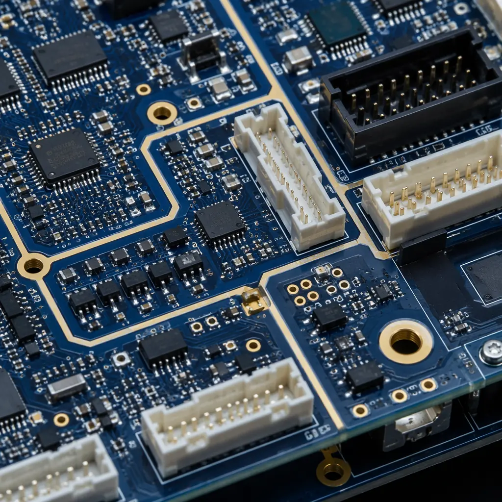
Design rule: Creepage distance between cells at different potentials must follow IEC 62109-1. For a 1,500V DC system (common in utility-scale BESS), the required creepage is ≥12mm at pollution degree 2. This often forces a slot in the PCB between high-voltage and low-voltage sections, a feature standard PCB design tools don't flag automatically.
Solar Inverter PCBs, DC-DC Conversion, Long-Term Outdoor Exposure
Solar inverters present a different PCB challenge: moderate power levels (3-10kW for residential, 50-250kW for commercial) but extreme longevity requirements. A residential solar inverter is expected to operate for 15-25 years with minimal maintenance, cycling daily from overnight lows to full-sun operating temperatures. Every thermal cycle stresses solder joints, laminate adhesion, and plated through-hole barrels.
The DC input stage of a string inverter handles 150-1,000V DC from the solar array. This stage uses aluminum-substrate PCBs (IMS, insulated metal substrate) for the boost converter section, where IGBTs or SiC MOSFETs dissipate 50-200W of heat. The thermal path is critical: junction → die attach → copper pad → dielectric layer → aluminum substrate → heatsink. The dielectric layer's thermal conductivity (typically 2-3 W/m·K for entry-level IMS, 5-8 W/m·K for high-performance) is the bottleneck.
Solar inverter PCB material selection trade-offs
| Substrate | Tg | Thermal Conductivity | Cost Multiplier vs FR-4 | Best For |
|---|---|---|---|---|
| High-Tg FR-4 (Shengyi S1000-2) | 180°C | 0.4 W/m·K | 1.5× | Control/logic boards |
| Aluminum IMS (Bergquist HT-07006) | 150°C (dielectric) | 2.2 W/m·K | 3× | Power stage, single-layer |
| Rogers 4350B + FR-4 hybrid | >280°C | 0.6 W/m·K | 8× | RF power + digital hybrid |
| Ceramic substrate (Al₂O₃ 96%) | N/A | 24 W/m·K | 15-20× | Highest power density, SiC modules |
For most residential and commercial inverters, the sweet spot is High-Tg FR-4 for control boards + single-layer aluminum IMS for power stages. This keeps total PCB cost under 8% of BOM while meeting 15-year life targets. We run this combination routinely at our Shenzhen factory, with automotive-grade process control (SPI before reflow, AOI after, X-Ray for BGAs) even when the end product isn't automotive.
Key Certifications for New Energy PCB Supply
New energy OEMs don't just ask for a certificate, they audit. Here are the certifications that procurement teams should verify, and what each one actually means for PCB quality:
IATF 16949:2016
Originally automotive, now the de facto quality standard for new energy. Requires process FMEA, control plans, and statistical process control (SPC) for every production step. If your PCB supplier has this, their defect prevention system is audited annually by a third party, not self-declared. Huaxing PCBA holds full IATF 16949 certification covering PCB fabrication and PCBA assembly.
UL Certification (UL 796 / UL 94 V-0)
UL 796 covers PCB base materials for flammability and electrical safety. UL 94 V-0 rating means the substrate self-extinguishes within 10 seconds, critical for battery-adjacent electronics. Verify the UL file number (we operate under E354321) and check it covers the specific laminate and copper weights you're specifying.
IPC-A-610 Class 3
Class 3 acceptance criteria require solder joints to meet tighter fillet dimensions, minimal voiding (<15% in BGA X-Ray), and zero defects that could cause field failure. Class 2 (standard industrial) allows occasional imperfections that Class 3 rejects. For BESS and solar inverters with 15+ year field life, Class 3 is the minimum acceptable standard.
ISO 14001:2015
Environmental management system certification. New energy OEMs increasingly require this as part of their Scope 3 emissions reporting. It verifies that the PCB facility manages chemical waste (etchants, plating solutions) responsibly, important for EU customers under CSRD requirements.
How to Qualify Your PCB Supplier for New Energy Projects
When evaluating PCB manufacturers for new energy products, standard supplier audit questions won't catch the risks that matter most. Here are five questions that expose whether a supplier actually understands new energy PCB production:
"What's your maximum copper weight, and how do you handle etch uniformity at 6oz?"
Heavy copper etching is non-trivial. At 6oz (210μm), the etch factor, the ratio of lateral etch to vertical etch, determines whether your 10mm trace is actually 10mm at the base. Suppliers who can't explain their etch compensation strategy don't actually run heavy copper in production.
"Can you show me your thermal shock test data for plated through-holes at 6oz?"
Thick copper barrels experience higher Z-axis expansion stress during thermal cycling. Reliable suppliers have IST (interconnect stress test) data showing <10% resistance change after 500 cycles from ambient to 260°C. If they can't produce this data, their heavy-copper vias are unvalidated.
"Do you perform partial discharge testing on high-voltage boards?"
For PCBs operating above 1kV, partial discharge (PD) testing per IEC 60270 detects voids in the laminate that will grow into short circuits over months of operation. Most PCB shops don't have PD test equipment, it's a 6-figure investment. If your supplier offers PD testing, they're serious about high-voltage applications.
"What's your minimum batch size for a hybrid stackup with Rogers and FR-4?"
Hybrid stackups (Rogers high-frequency layers bonded to FR-4 structural layers) require different lamination cycles and CTE management. Suppliers who quote 1-panel minimums for hybrids either don't understand the process complexity or are absorbing massive yield losses they haven't told you about. Realistic minimums are 10-20 panels.
"Walk me through your conformal coating inspection process."
Conformal coating on high-voltage PCBs is a safety feature, not cosmetic. Proper inspection requires UV light (for UV-tracer coatings) and thickness measurement at specified test coupons. If the supplier says "visual inspection" without mentioning UV or thickness gauges, their coating process is unverified.
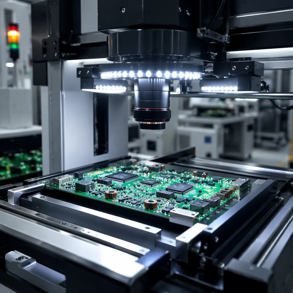
The new energy sector is the fastest-growing segment of the PCB industry, but it's also where the gap between "can quote" and "can deliver" is widest. A supplier that handles 2oz FR-4 for consumer products may quote your 6oz Rogers hybrid BMS board, but their yields will tell a different story. The questions above separate the shops that have invested in new energy production capability from those that are hoping you won't ask.
At Huaxing PCBA, new energy PCB production runs on our 8 dedicated SMT lines with IATF 16949 process controls, 6oz copper capability, and ISO 14001 environmental management. Our engineering team speaks English, reviews Gerber files within 4 hours, and delivers prototypes in 3 days. Send your specs, we'll tell you honestly whether we're the right fit.
