
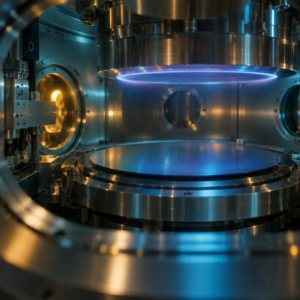
A thin-film deposition tool is one of the more demanding environments an industrial control board can be asked to survive. The chamber runs at pressures in the 10-6 mbar range, and at that pressure every polymer in the system is quietly releasing gas. The circuit board that drives the RF generator, the substrate heater or the gas delivery manifold sits directly in that environment or immediately behind it — and the ordinary assumptions that govern industrial PCB specification stop applying. A board that would be entirely adequate in a factory cabinet can, in a deposition tool, be the single largest source of the water vapour and hydrocarbon background that ruins film quality.
This guide is written for the buyer side: equipment engineers and supply-chain managers at semiconductor capital-equipment OEMs qualifying a PCB partner for vacuum-process electronics. It covers why deposition tool boards are specified differently, how outgassing becomes a contamination budget, which materials survive vacuum and thermal cycling, and a supplier qualification checklist built specifically for this application. Our own production runs across 32 layers with IPC Class 3 acceptance and ionic cleanliness verification, and the requirements below reflect what vacuum-grade electronics actually demand.
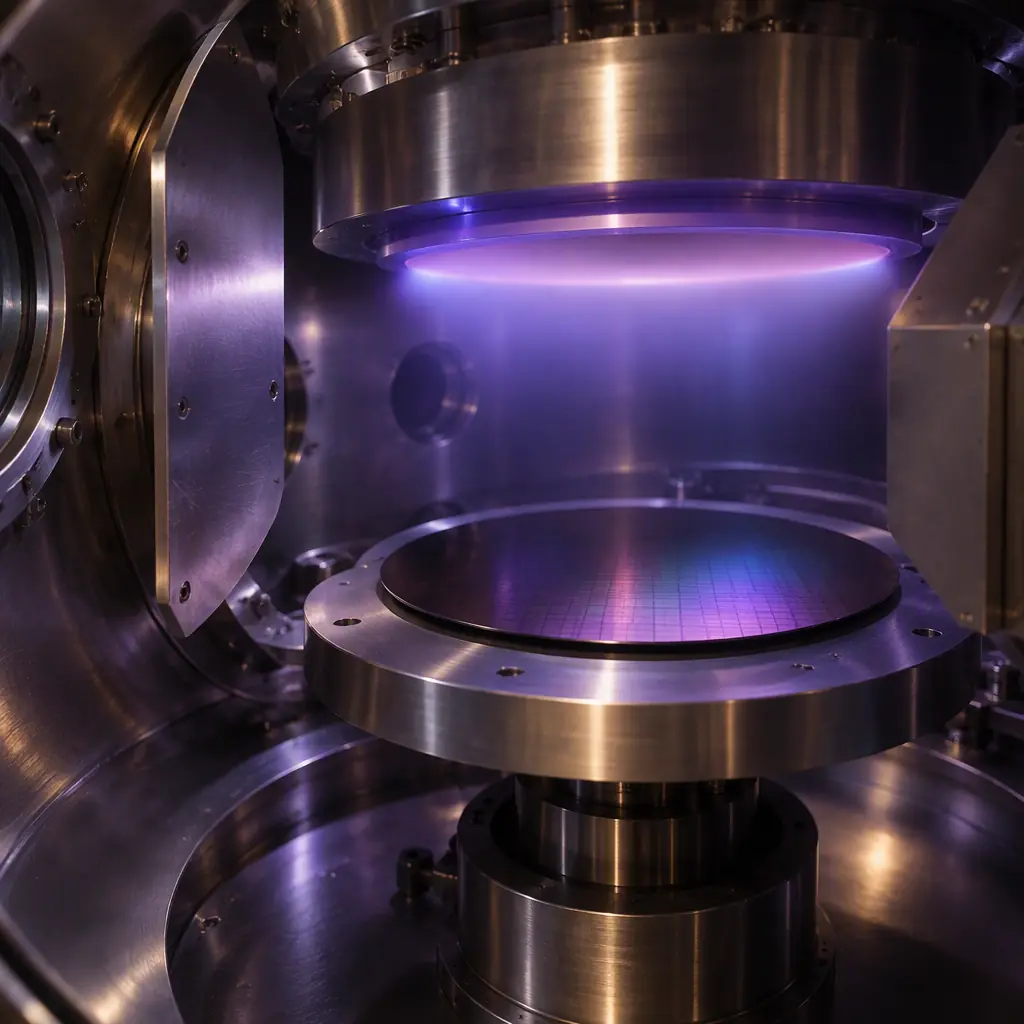
Why Deposition Tool Electronics Are Not Ordinary Industrial Boards
Most industrial control electronics are specified against three things: electrical performance, thermal limits and mechanical durability. Deposition tool electronics are specified against a fourth, often dominant requirement — the board must not contaminate the process. This inverts the normal design hierarchy. A material that offers excellent dielectric performance but releases volatile organics under vacuum is disqualified, regardless of how good its electrical numbers are.
The practical consequence is that the same board specification that works in the load-lock control cabinet may be unacceptable on the chamber-side electronics, even though both drive similar circuits. Buyers who source from a general industrial PCB supplier frequently discover this late, when the tool passes electrical test but fails a chamber qualification or a residual gas analysis check. The failure mode is not a broken board — it is a contaminated process, and it appears as film defects, adhesion problems or a base pressure that will not reach specification.
| Requirement | Standard industrial PCB | Deposition tool electronics |
|---|---|---|
| Primary performance driver | Electrical and thermal | Contamination and vacuum survival |
| Material selection basis | Cost, Dk/Df, Tg | Outgassing rate, vacuum stability, then electrical |
| Cleanliness | Cosmetic, functional | Quantified ionic and particulate limits |
| Pre-delivery process | Test and pack | Test, clean, document bake, vacuum-compatible pack |
| Acceptance standard | IPC Class 2 typical | IPC Class 3 with cleanliness records |
What changes for the buyer: you are no longer purchasing a board that meets an electrical specification. You are purchasing a board plus a documented cleanliness and outgassing history, and the second part is where most supply chains are thin.
Outgassing, Virtual Leaks and the Contamination Budget
Outgassing is the release of adsorbed and absorbed volatiles from materials under vacuum. In an atmospheric-pressure application, those molecules simply diffuse into the room and nobody notices. In a sealed chamber, they accumulate until the pump can carry them away, and that accumulation sets a floor on achievable base pressure. Water vapour is the dominant species by volume in most systems, followed by hydrocarbons from machining oils, plasticisers and polymer residues. For a deposition tool, hydrocarbon background is the more damaging of the two because it incorporates directly into growing films.
The framework buyers should use is a contamination budget rather than a pass/fail claim. Each assembly in the chamber contributes some mass loss; the sum must remain below what the pump and process can tolerate. That is why "vacuum compatible" as a marketing phrase means nothing — the question is always which material, at what surface area, baked to what schedule, contributing how much. The two reference points worth knowing are ASTM E595, the standard total mass loss and collected volatile condensable materials test used across aerospace and vacuum industries, and IPC-TM-650 methods for evaluating laminate and coating behaviour. Ask your supplier which of these they have actually run.
| Contamination source | Where it comes from | How it is controlled |
|---|---|---|
| Water vapour | Laminate absorbed moisture, plating residues | Bake schedule before installation; dry storage and vacuum packing |
| Hydrocarbons | Machining oils, plasticisers, flux residue, adhesives | Cleaning and verification; adhesive and label selection |
| Virtual leaks | Trapped volumes under components, blind holes, unbaked solder joints | Via and hole design review; vent paths; assembly process control |
| Particulates | Drilling and routing debris, handling | Class 3 cleaning, controlled handling, cleanroom packing |
| Sublimation from coatings | Conformal coating and marking inks | Coating family selection; cure verification |
A virtual leak deserves particular attention because it is invisible in a datasheet and entirely a design-and-process issue. A blind threaded insert, a component body sitting over an unvented pocket, or a via that is plated shut at one end can hold a trapped volume that bleeds out slowly over hours or days of pumping. The chamber will pump down, then plateau at a pressure worse than expected, and the cause is a mechanical trapping feature rather than a material. This is a design review item, not a purchasing one — but the buyer is the one who suffers the schedule impact when it is discovered during tool integration.
Material Selection for PVD, CVD and ALD Control Electronics
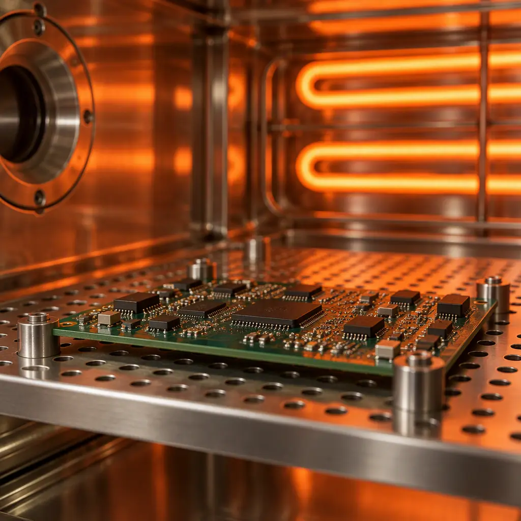
Material selection for vacuum electronics is a two-stage filter. First, eliminate anything with known high outgassing or poor vacuum stability. Second, select from the survivors on electrical and thermal grounds. In practice, three laminate families cover most deposition tool requirements, and the choice is driven by temperature, layer count and cost rather than by preference.
| Material | Typical Tg | Best fit | Trade-off |
|---|---|---|---|
| Standard FR-4 (mid/high Tg) | 150-180°C | Chamber-external control boards, load-lock electronics | Lowest cost; needs documented bake; watch absorbed moisture |
| Polyimide | 250°C+ | Heater control, high-temperature zones, multi-layer stacks | Higher cost, higher moisture uptake, needs longer bake |
| Ceramic / ceramic-filled | n/a | Very high pin count, extreme thermal stability | Significantly higher cost; limited panel size; CTE management |
| PTFE / RF laminates | n/a | RF generator and matching network electronics | Mechanical softness; requires specialised processing |
For most deposition tool control electronics, high-Tg FR-4 is the right answer for anything outside the hot zone, and polyimide or a ceramic solution takes over where temperature and via reliability demand it. The mistake to avoid is over-specifying polyimide everywhere "because vacuum" — polyimide absorbs more moisture than FR-4 and needs a longer bake to reach the same background level. A supplier who reflexively recommends polyimide for every vacuum board is optimising for the look of the specification rather than the measured outcome.
Copper weight and stackup matter less for vacuum than for power electronics, but layer count interacts with bake time: a thicker, more layered board holds more absorbed moisture and needs a correspondingly longer bake schedule. If the tool's installation window is tight, this is worth surfacing during supplier selection rather than at the end of build. For boards that also carry heavy current in the chamber, our guide to heavy copper PCB fabrication covers the interaction between copper weight and stackup.
Cleanliness, Particulate and Class 3 Requirements
Cleanliness in vacuum electronics is a specification, not a habit. The relevant acceptance standard is IPC Class 3, which is written for products where continued performance is critical and where failure cannot be economically recovered — semiconductor capital equipment falls squarely inside that definition. Class 3 is enforced primarily through tighter acceptance criteria, but the buyer should care about the process controls that make it achievable: solder joint inspection under magnification, cleaning verification, and documentation.
The measurable cleanliness parameter is ionic contamination, reported in micrograms of sodium chloride equivalent per square centimetre. Post-cleaning limits in the low fractions of a microgram per square centimetre are the target for boards headed into critical environments. Residue that would be benign in a ventilated cabinet becomes an active problem in a sealed chamber, because there is nothing to carry the ionic species away and no way to clean the board after installation.
Require ionic contamination data, not a cleaning claim
Ask for the measured value per board lot against an agreed limit. "Cleaned" without a number from a documented test method tells you nothing about the delivered boards, only about the existence of a cleaning machine.
Specify IPC Class 3 acceptance explicitly
Class 2 is the default for most industrial work. Vacuum-process boards should be contracted at Class 3, with the acceptance criteria applied at inspection rather than only at final test. The differences that matter most are in plated-through-hole quality, annular ring and surface finish integrity.
Control particulate from handling onward
A chemically clean board handled on an open bench is no longer clean. Cleanroom packing, glove and garment discipline and particulate-controlled routing are part of the deliverable. See our guide to cleanroom classification to ISO 14644 for how the class numbers map to handling requirements.
Ask how cleanliness is verified, and how often
A verification method without a sampling frequency is theatre. The defensible answer is a named test method applied on a defined frequency per lot, with results retained and available to you. Our ionic contamination testing guide covers the methods and their limits.
Thermal Cycling Inside the Tool: Where Boards Fail
Temperature is the second axis of difficulty. Deposition tools cycle between process temperature and ambient repeatedly, and the electronics bolted to a heated stage or a chamber wall see a substantial portion of that swing. The failure modes that emerge are not the ones a standard reliability test screens for.
Plated through-hole barrel cracking
Repeated expansion and contraction of the laminate against a rigid copper barrel is the classic through-hole fatigue mechanism. It is accelerated when the board is thick, the hole is small and the temperature swing is large — precisely the profile of a deposition tool control board. Copper thickness uniformity in the barrel is what buys margin.
Via fatigue under high-cycle service
Boards that see many shallow cycles fail differently from those that see few deep ones. Via reliability under thermal cycling is measured with IST or thermal shock testing rather than temperature-humidity soak, and the results are not interchangeable. Our IST vs thermal shock comparison explains which test answers which question.
Delamination at the laminate-to-copper interface
Hydrolytic degradation from absorbed moisture, followed by thermal excursion, causes separation at the resin-to-copper interface. It appears as measling or blistering and is directly linked to the moisture the board absorbed before the bake that was supposed to remove it. Pre-bake and storage discipline is the control.
Component and solder joint stress at the interface
Large components with low thermal expansion mounted on a laminate that expands more will stress their joints every cycle. The boards that survive are the ones where the design accounted for the mismatch rather than relying on underfill alone. Where the joint needs reinforcement, our underfill selection guide covers the material choices.
Supplier Qualification Checklist for Vacuum-Grade Electronics
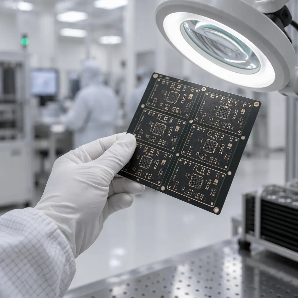
The checklist below is written for the buyer qualifying a PCB partner for deposition tool electronics. Each item is answerable with a document, a number or a named process. An answer that consists of an assurance rather than an artifact is a gap to close before you commit a tool schedule.
Which cleanliness standard and limit applies, and who sets it?
Expect a named test method and a numeric limit in micrograms of NaCl equivalent per square centimetre, agreed with you rather than chosen by the supplier alone.
What is the bake schedule, and is it documented per lot?
The schedule should specify temperature, duration and the point in the process at which it happens, with a record delivered alongside the boards. A bake that is described but not recorded cannot be relied on.
Which outgassing data exists for the materials specified?
For critical assemblies, require material-level outgassing data rather than a blanket compatibility statement. ASTM E595 or equivalent data on the laminate, coating and adhesive families is the defensible evidence.
How are virtual leaks designed out?
Ask for the design review that covers trapped volumes, blind holes and unvented component pockets. Confirm the manufacturer flags these during DFM rather than after a failed pump-down.
Is Class 3 acceptance applied at inspection or only at final test?
Class 3 requires tighter criteria at the inspection stages that catch hole quality and annular ring defects. Final electrical test will not surface them.
What is the packing and shipping specification?
Vacuum-compatible packaging, moisture barrier bags with desiccant, and a documented exposure window after opening. A clean board shipped in open foam has been re-contaminated before it reaches your dock.
Summary and Next Steps
Deposition tool electronics are specified on a different axis from ordinary industrial boards. The dominant requirement is that the assembly not contaminate the process, and that requirement reaches into laminate choice, bake schedule, cleaning limits, via design and packing. Material selection narrows quickly once outgassing is treated as a first-order filter, and the remaining decisions — high-Tg FR-4 versus polyimide versus ceramic — come down to temperature and layer count rather than preference. The buyer's job is to convert "vacuum compatible" into numbers on a purchase specification, and to require the records that prove the numbers were met.
At Huaxing PCBA we build vacuum and semiconductor equipment electronics up to 32 layers with IPC Class 3 acceptance, with documented cleaning verification and bake schedules available per lot. Our facilities hold IATF 16949 and ISO 9001 certification. Read our semiconductor fab equipment PCB guide or send your Gerber and BOM for a vacuum-grade review — free DFM feedback and a quote within 24 hours.
