
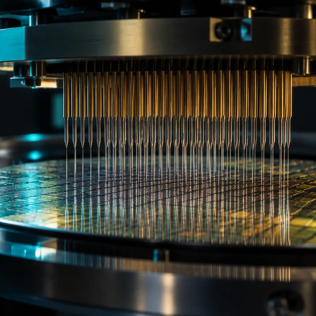
When a probe card fails to meet contact resistance or a device interface board will not hold its impedance through the pogo field, the root cause is usually decided long before either was built — at the moment the test specification was converted into a fabrication drawing. Probe cards and ATE interface boards sit at the awkward intersection of semiconductor tolerances and printed circuit board processes. The pin counts are comparable to a package substrate, the pitches reach below the typical PCB fine-line limit, and the electrical requirements assume a controlled-impedance environment throughout. Each of those pressures lands on the fabricator, and the buyer who understands the mapping can tell early whether a supplier is genuinely capable or merely willing.
This guide is written for test engineering and procurement teams sourcing probe card substrates and ATE interface electronics. It covers what these boards do, how pin count and pitch translate into fabrication limits, the signal integrity budget that has to survive the transition from tester to device, and a qualification checklist for the substrate supplier. Our own capabilities reach 32 layers with HDI and via-in-pad filling, and the limits discussed below reflect where the process boundaries actually sit.
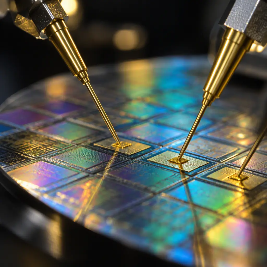
What a Probe Card and an ATE Interface Board Actually Do
A probe card is the mechanical and electrical interface between a wafer prober and the individual die on the wafer. It carries an array of fine probes that contact the die's pads, and it routes those connections back to a printed circuit board that presents a standardised interface to the tester. An ATE device interface board — sometimes called a load board or DIB — performs the equivalent function at package level, carrying a socket field on one side and the tester interface on the other, often with substantial active circuitry built in.
Both are printed circuit boards in the literal sense, and neither behaves like a conventional board. The probe card substrate is usually the smallest and most densely routed part of the entire test system, and it is the part that wears. An interface board sees repeated insertion cycles, thermal excursions as the handler moves parts between hot and cold test, and the mechanical load of a socket array that may carry thousands of contacts. The electrical environment is uncompromising because the tester's measurement bandwidth depends on the integrity of the path through these boards.
| Characteristic | Probe card substrate | ATE interface / DIB |
|---|---|---|
| Primary interface | Probe needles to die pads | Socket field to packaged device |
| Typical pin count | Hundreds to several thousand | Hundreds to several thousand |
| Dominant constraint | Pitch and planarity at the probe field | Impedance, layer count and power delivery |
| Service life | Consumable — replaced on wear | Long-life with rework and socket replacement |
| Substrate options | Ceramic, high-density PCB, hybrid | High-Tg FR-4, polyimide, hybrid stacks |
What changes for the buyer: you are not specifying a generic board with a high pin count. You are specifying a substrate whose routing density, impedance control and mechanical stability all have to hold simultaneously, and where a small shortfall in any one of them shows up as yield loss on your test floor rather than as an obvious defect.
Pin Count, Pitch and the Fabrication Limits They Force
The single most useful number when evaluating a probe card substrate quotation is the escape pitch at the probe field. Every other fabrication parameter follows from it. A device with a fine-pitch pad array forces a routing density at the probe field that must be reduced to something the board can carry away, and the mechanism for doing that is layer count, via type and line geometry.
| Probe field pitch | Practical routing approach | Layer count pressure |
|---|---|---|
| Above 150 µm | Direct escape, standard fine-line traces | Moderate |
| 100-150 µm | Fine-line escape, some via-in-pad | High |
| 75-100 µm | HDI with microvias, sequential lamination | Very high |
| Below 75 µm | Ceramic or thin-film routing at the field | Extreme — often hybrid construction |
Two fabrication limits dominate beyond the pitch. The first is line width and spacing: reducing trace geometry to escape a dense field also reduces the process window, and yield falls non-linearly as the geometry tightens. The second is via geometry, and in probe card work the critical metric is aspect ratio — board thickness divided by drilled hole diameter. A thick board with small vias is harder to plate uniformly, and poor plating uniformity in the barrel is what later becomes an intermittent open under thermal load.
Get the escape pitch in writing before the quote
Ask the supplier to state the pitch the design requires and the minimum they can produce with acceptable yield. A quote issued without that number has not been evaluated against the design — it has been priced.
Ask for the aspect ratio being quoted
Thickness and hole size together define difficulty. An 8:1 quote and a 12:1 quote are different products. The substrate stackup should be chosen so the aspect ratio stays inside a proven process rather than at the edge of one.
Confirm the via treatment at the probe interface
Via-in-pad with conductive or non-conductive filling, followed by planarisation, is what allows a component or probe pad to sit directly over a via without solder wicking or an uneven surface. In probe card work the planarity requirement is tighter than for ordinary assembly — see our guide to PCB via technology for the process variants.
Check whether castellated features are needed
Where the substrate must present edge contacts to a mating element, castellation and edge plating bring their own tolerance stack. Our castellated holes and edge plating guide covers the design rules that keep them manufacturable.
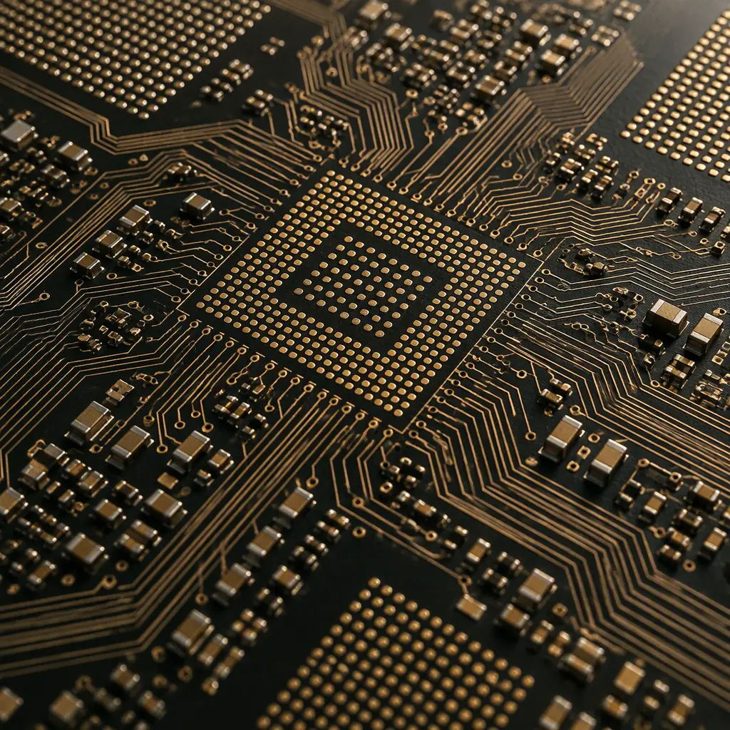
Signal Integrity on a DIB: Impedance, Loss and Crosstalk
An ATE interface board is a transmission path, and it has to preserve the signal well enough for the tester to make its measurement. The three parameters that matter are characteristic impedance, insertion loss and crosstalk. All three worsen as the board gets longer, more layered and more densely routed around a socket field, which is exactly the direction interface boards trend.
Impedance control starts with the stackup. The dielectric thickness between a trace and its reference plane, the trace geometry and the dielectric constant of the laminate together set the characteristic impedance, and it holds only if the reference plane is continuous beneath the trace. A plane split or a reference change mid-route turns a controlled-impedance trace into an uncontrolled one. In a DIB, where power and ground planes are interrupted by socket via fields, maintaining continuous references is a genuine layout effort rather than an automatic consequence of specifying 50 ohms. Our impedance control guide covers the stackup and tolerance aspects in more detail.
| Parameter | Why it matters on a DIB | What controls it |
|---|---|---|
| Characteristic impedance | Mismatch at the pogo or socket boundary causes reflection | Stackup, trace geometry, continuous reference plane |
| Insertion loss | Reduces eye height and shrinks the tester's margin | Trace length, dielectric loss, surface finish, via count |
| Crosstalk | Couples fast edges into adjacent channels | Trace separation, ground referencing, layer assignment |
| Return path continuity | Broken returns radiate and distort | Via stitching, plane integrity, connector ground strategy |
| Socket and pogo transitions | Often the dominant contributor to total loss | Component selection and the transition design around it |
The point to take into a supplier conversation is that impedance-controlled fabrication is a capability claim that should come with evidence, not an adjective. The defensible evidence is a stackup drawing with the target impedance and tolerance stated per layer, and test-coupon data showing measured values. High-speed test channels push the requirement further — where the DIB is carrying the same class of signalling discussed in our guide to 112G and 224G SerDes design, loss budget management becomes the dominant design effort rather than a secondary consideration.
PCB Substrate vs Ceramic: Choosing for Pin Count, Cost and Life
Probe card substrates are built on either an organic PCB stackup, a ceramic substrate, or a hybrid that uses fine-line ceramic or thin-film routing at the probe field and a conventional PCB for the fan-out and interface. The choice is not about which is better in the abstract — it is about which constraint binds hardest in a given application.
| Consideration | High-density PCB substrate | Ceramic substrate |
|---|---|---|
| Fine-line capability | Good with HDI; limited below ~50 µm | Excellent, well into thin-film territory |
| Panel size and layer count | Large panels; high layer counts routine | Smaller format; layer count more constrained |
| Thermal expansion | Higher CTE; needs management at the interface | Low CTE, closer to silicon |
| Cost at moderate density | Lower | Substantially higher |
| Repair and rework | Generally easier | Limited |
| Best fit | Volume production test, larger interface boards, cost-sensitive programs | Extreme pitch, high-temperature test, low-CTE requirements |
The hybrid route is common and often the right answer: use the substrate technology where its advantage is realised and the conventional board where it is cheap and plentiful. For a buyer, the practical implication is that the substrate supplier and the PCB supplier may be different organisations, and the integration tolerance between them has to be owned by someone. Our overview of ceramic, PTFE and polyimide substrates covers the material-level comparison that sits underneath this decision.
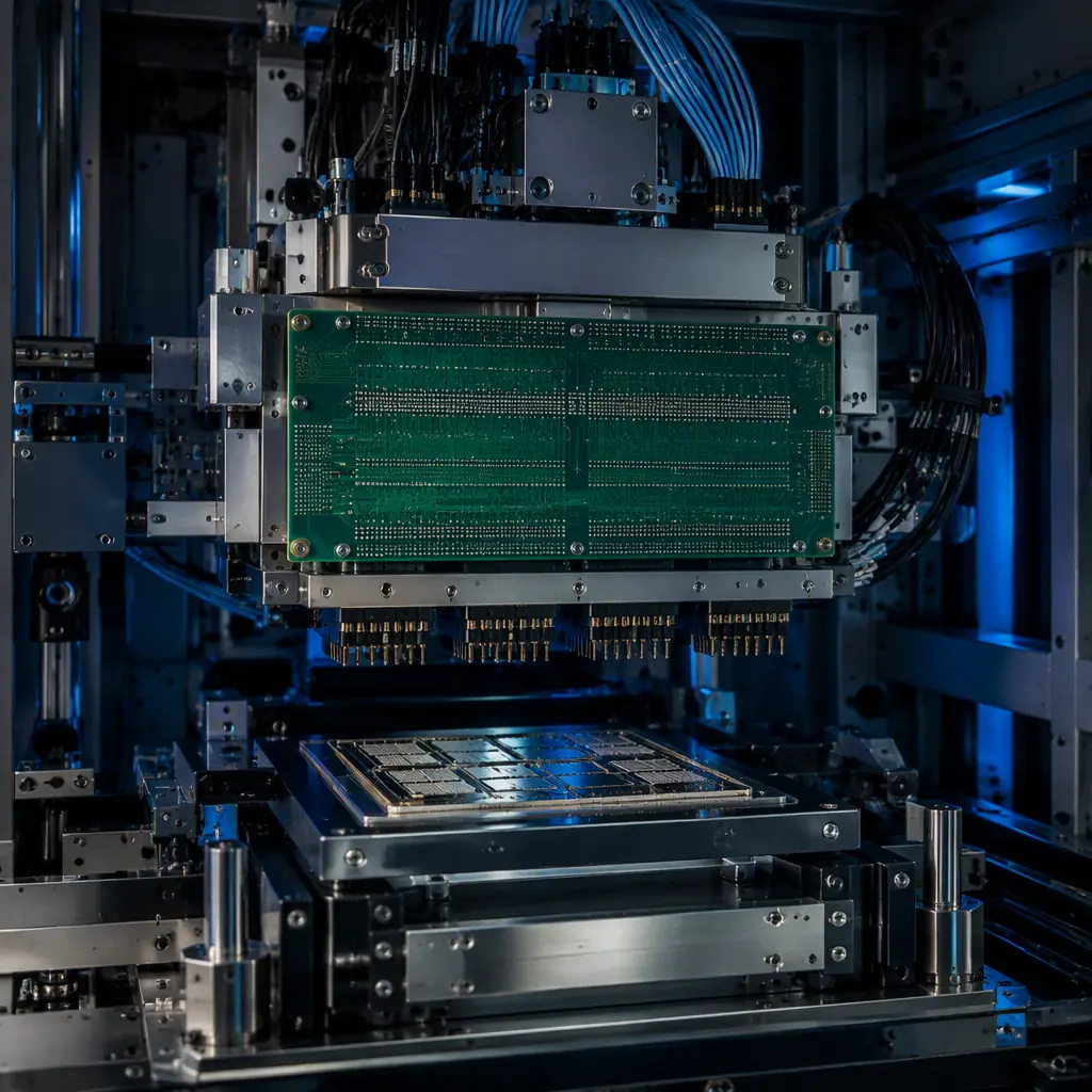
Thermal and Mechanical Load in a Test Environment
An interface board lives in a mechanically hostile place for a piece of electronics. It is inserted and removed repeatedly, clamped against a socket field and a tester interface, and cycled between hot and cold test conditions. Three failure mechanisms follow from that and should be reflected in the specification.
Planarity across the socket field
A socket array makes contact across a large area, and any bow or twist in the board translates directly into contact force variation — some contacts over-stressed, others not making reliable contact. Board thickness tolerance, layer balance and mechanical stiffening all feed into planarity, and it must be specified rather than assumed.
Repeated insertion cycle durability
Connector and interface features wear with every insertion. The board-level controls are plating thickness at the interface, surface finish selection and mechanical support around the connector zone. This is a specification item for mating features, not an afterthought.
Thermal cycling between hot and cold test
Multi-temperature test cycles the board repeatedly, and the same via and through-hole fatigue mechanisms apply as in any thermal-cycled electronics. Where the board must hold performance across many cycles, qualification should be by a cycling test rather than a soak — our IST vs thermal shock comparison explains which test measures which failure mode.
CTE management at the interface to socket and probe hardware
Where a low-expansion element is mounted on a higher-expansion laminate, every thermal cycle stresses the joint between them. Underfill, stiffeners and material selection all contribute. Our underfill selection guide covers the material option where the mismatch has to be absorbed at the joint.
Twist and bow tolerance specified against the application
IPC default bow and twist limits are written for general electronics. A socket field needs a tighter number, and it should appear explicitly on the fabrication drawing with the measurement method defined.
Supplier Qualification Checklist for Probe Card Substrates
Use the following when qualifying a fabrication partner for probe card or interface board work. Each question has a specific, checkable answer, and a supplier who handles this class of work will produce the evidence without preparation.
What is your minimum line width and spacing on the quoted stackup?
Expect a number tied to a yield statement, not a theoretical minimum. The geometry the design needs should sit inside a proven process window rather than at its boundary.
What aspect ratio is achievable on that stackup, and with what plating uniformity?
Ask how barrel copper thickness uniformity is verified. Backlight testing and cross-section inspection are the evidence; a specification statement alone is not.
Can you supply a stackup with stated impedance targets and tolerance per layer?
The stackup drawing should show target impedance, tolerance and the material used. Measured test-coupon results close the loop.
How is via-in-pad filled and planarised?
Filling type — conductive or non-conductive — matters for thermal performance, and planarisation quality determines whether a probe pad or component can sit over the via reliably. Ask for the process and the inspection criterion.
What bow and twist can you hold on a board this size?
A measured figure with the gauge method, not the IPC default. This is the parameter most likely to be discovered late if it is not specified early.
What acceptance class and inspection level apply, and is it applied in-process?
Probe card substrates belong at IPC Class 3, and the criteria should be applied at the plating and drilling inspection stages rather than only at final electrical test. Our IPC Class 2 vs Class 3 comparison covers where the standards differ.
Who owns integration tolerance if the substrate is a hybrid build?
Where fine-line routing and conventional PCB processes come from different suppliers, the interface between them needs a single owner for dimensional and electrical tolerance. Identify that owner before the design is released.
Summary and Next Steps
Probe card and ATE interface boards are specified by translation: pin count and pitch set the routing density, routing density sets the line geometry, via type and layer count, and the electrical requirement sets the stackup and impedance tolerance. The buyer's leverage comes from surfacing that translation early — obtaining the escape pitch, the aspect ratio and the impedance targets in writing before a purchase order, and requiring evidence that the process window has been demonstrated rather than asserted. Substrate technology choice between organic PCB, ceramic and hybrid then follows from which constraint actually binds in the application, not from a general preference.
At Huaxing PCBA we fabricate high-density interface and test substrates up to 32 layers with HDI, via-in-pad filling and impedance control to stated tolerances, with Class 3 acceptance available. Our facilities hold IATF 16949 and ISO 9001 certification. Read our guide to ATE and semiconductor test boards or send your substrate requirements for a capability review — free DFM feedback and a quote within 24 hours.
