
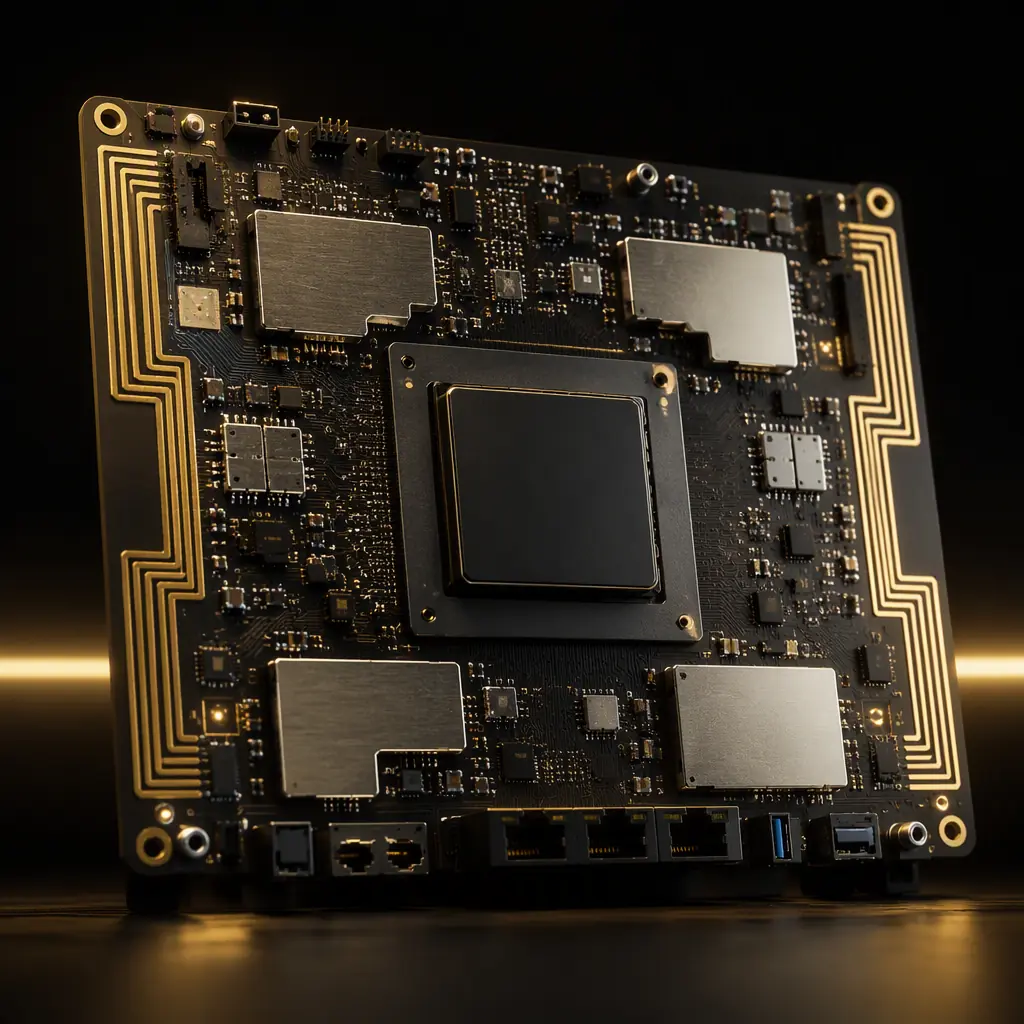
Wi-Fi 7 (802.11be) and Wi-Fi 6E are the first Wi-Fi generations to use the 6 GHz band — 5925–7125 MHz depending on region — and that single change moves the RF design problem from "route it reasonably" to "the board is part of the antenna and the filter." At 6 GHz, a 10 mm trace carries meaningful loss, a via stub is a resonant structure, and the tolerance on your laminate's dielectric constant directly sets how far from 50 Ω your real traces land.
Huaxing PCBA builds Wi-Fi 6E/7 boards for routers, gateways, and IoT access points — up to 32 layers with ±5% impedance control, back-drilling for high-layer-count designs, and low-loss laminate processing (Rogers, Megtron, PTFE) alongside standard FR-4. This guide covers the layout rules that determine real throughput, the material decisions that control cost, and the certification checks — including SRRC for China-bound products — that every Wi-Fi 7 design eventually faces.
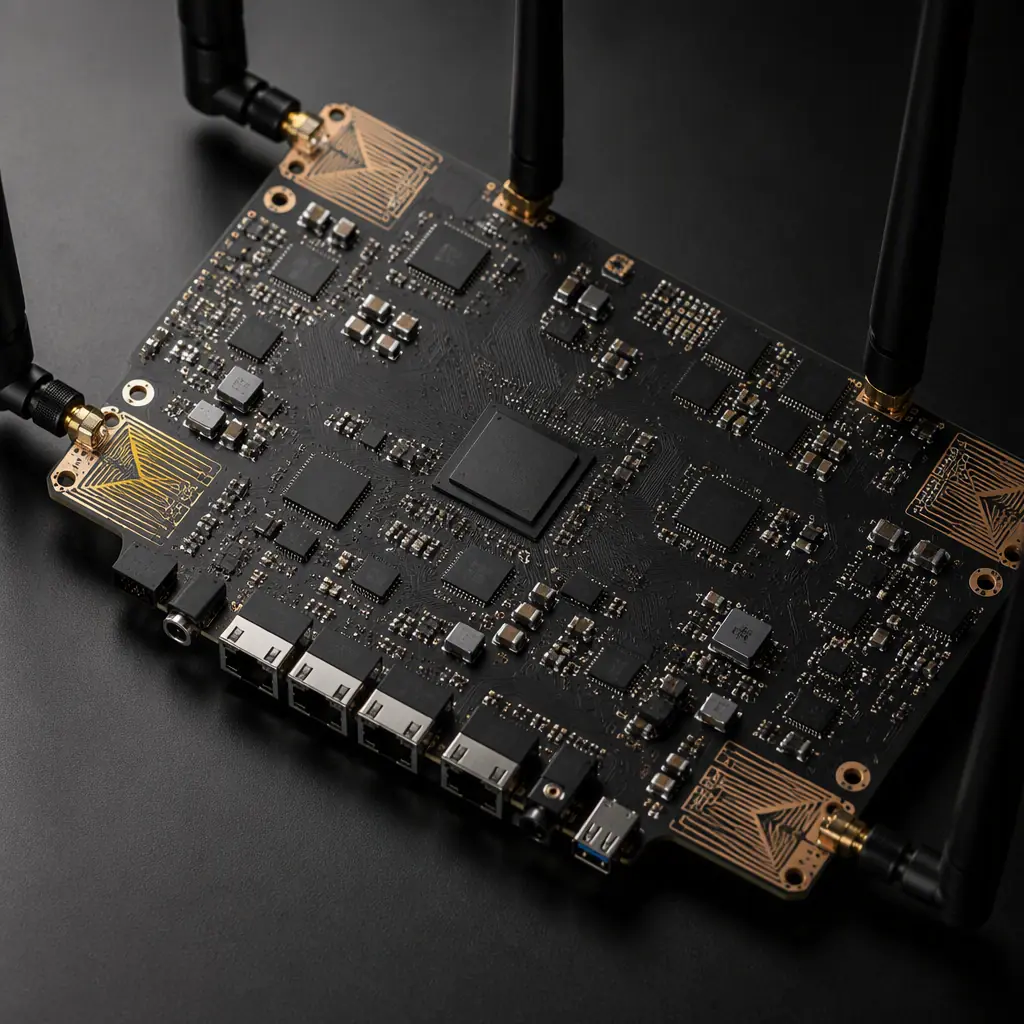
Does Wi-Fi 6E/7 PCB Design Require Rogers or Other Low-Loss Materials?
Not always — and knowing when it does is where most of the cost gets saved. At 6 GHz, standard FR-4's dissipation factor (Df ≈ 0.018–0.022) causes insertion loss roughly three times higher than at 2.4 GHz. For a short antenna feed under one inch, FR-4 with strict impedance control is usually acceptable. But for longer RF traces — the front-end path from SoC to the antenna switch, or the transmit path of a high-power AP — the loss budget forces a low-loss laminate.
| Material | Dk (typ.) | Df (typ. @ 10 GHz) | Relative Cost | Typical Role |
|---|---|---|---|---|
| Standard FR-4 | 4.2–4.5 | 0.018–0.022 | 1× | Digital layers, short feeds |
| Low-loss FR-4 (e.g., Shengyi S1000-2M) | 4.2–4.4 | 0.008–0.010 | 1.2–1.5× | Affordable RF compromise |
| Megtron 6 / 7 | 3.6–3.7 | 0.002–0.003 | 3–4× | High-layer-count, high-data-rate boards |
| Rogers RO4003C | 3.38 | 0.0027 | 5–8× | Antenna feeds, RF front ends |
| PTFE (Rogers RT/duroid, Taconic) | 2.2–3.0 | 0.0009–0.002 | 8–15× | Highest performance, antenna substrates |
The engineering answer is almost always a hybrid stackup: FR-4 or low-loss FR-4 for the bulk of the board, with a Rogers or Megtron layer pair only where the RF traces run. Hybrid laminates cost more per panel and add processing steps (plasma treatment, different drill parameters), so the goal is to confine the expensive material to the traces that need it. Our laminate selection guide walks through the trade-offs per application, and the PTFE manufacturing guide covers the processing constraints of the top-tier materials.
Key Takeaway: "Wi-Fi 7 needs Rogers" is wrong as a blanket statement. Short feeds on FR-4 with tight impedance control pass easily; long RF paths and high-power transmitters need low-loss laminates. Design the hybrid stackup around the actual trace lengths and power levels.
Impedance at 6 GHz: What ±5% Actually Means at the Fab
Every Wi-Fi RF trace is designed to 50 Ω (and differential pairs to 100 Ω), but the fabricated value is a distribution, not a point. The practical question is how wide that distribution is — and it is set by three variables the layout engineer controls only indirectly: the laminate's Dk tolerance, the etch process, and the dielectric thickness tolerance.
Understand the Dk Tolerance Chain
A laminate with Dk specified at 4.3 ± 0.2 shifts trace impedance by roughly ±2–3% on its own. Stack that on top of etch and thickness variation, and the honest fabrication capability for controlled impedance is ±10% on standard FR-4 — the ±5% you see in datasheets refers to a controlled process with selected materials and impedance coupons on every panel. If your design truly needs ±5%, say so explicitly and expect the fab to run tighter process controls.
Account for Etch Compensation and Copper Roughness
At 6 GHz, copper surface roughness contributes measurable loss — a standard electrodeposited (ED) foil can add 20–30% more loss than low-profile (LP) foil at these frequencies. Specify LP foil for the RF layers, and let the fab apply etch compensation so the final trace width lands at the target, not the drawn width. Our manufacturing tolerances guide covers etch, drill, and registration limits in detail.
Require TDR Coupon Verification — Measured, Not Designed
Never accept "designed to 50 Ω." The impedance coupon on each panel must be TDR-measured, and the report should show the measured value per coupon. A fab that returns measured data is controlling its process; a fab that returns the design value is copying it from the order form. Our impedance control guide has the coupon specification template.
6 GHz Routing: Return Paths, Via Stubs, and Back-Drilling
Above 5 GHz, the return current hugs the trace — it does not spread out the way it does at low frequency. That makes the reference plane immediately beneath every RF trace the most important routing constraint on the board.
Never Route an RF Trace Over a Plane Split
A split in the ground or power plane under an RF trace forces the return current to detour, which adds inductance, creates radiation, and distorts the impedance. Keep RF traces over a continuous ground reference for their entire length. If a plane split is unavoidable, stitch the two sides with capacitors sized for the band (e.g., 100 pF at 6 GHz) at the crossing point.
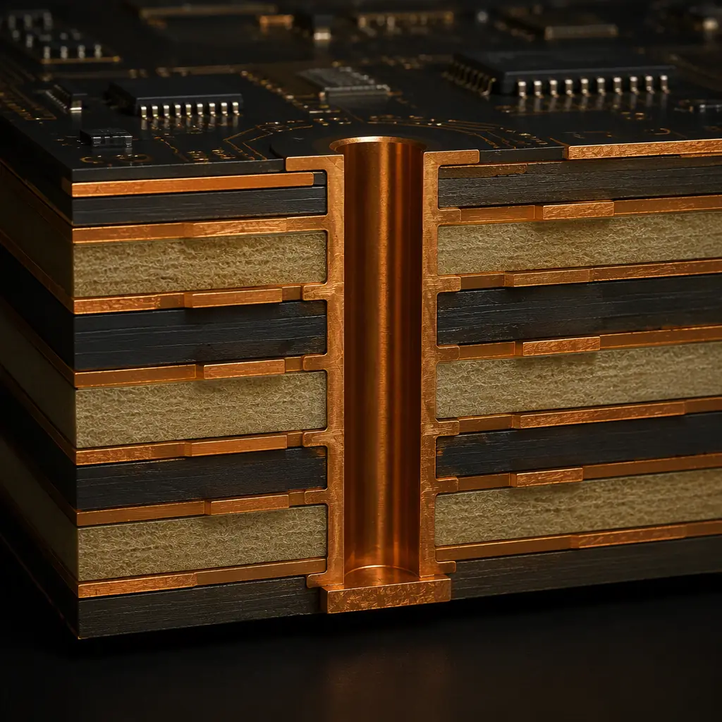
Via Stubs Are Resonators at 6 GHz — Back-Drill or Skip
A through via that continues past the routing layer leaves a stub of plated barrel. At 6 GHz, a 1 mm stub has a noticeable reactance and can resonate inside the band; a 2 mm stub can swallow several dB at specific frequencies. Options: route RF on the outer layers to avoid vias entirely, use blind/buried vias in an HDI stackup, or back-drill the stubs. Back-drilling adds a process step and cost, so it belongs only on the critical RF nets — our back-drilling guide explains when it pays for itself.
Stitch Ground Along the RF Path
Ground vias flanking an RF trace confine the fields, reduce coupling, and give return current a low-impedance path at layer transitions. A rule of thumb for 6 GHz: ground vias every 1–2 mm along coplanar-waveguide RF traces, and a via right beside every RF via that changes layers. Our signal integrity guide covers via stitching and return-path discipline in depth.
Antenna Keep-Out and Multi-Radio Coexistence
Wi-Fi 7 access points are multi-radio systems: 2.4 GHz, 5 GHz, and 6 GHz radios, often alongside Bluetooth and sometimes Zigbee. Each antenna needs its zone, and the zones need isolation from each other and from the board's digital noise.
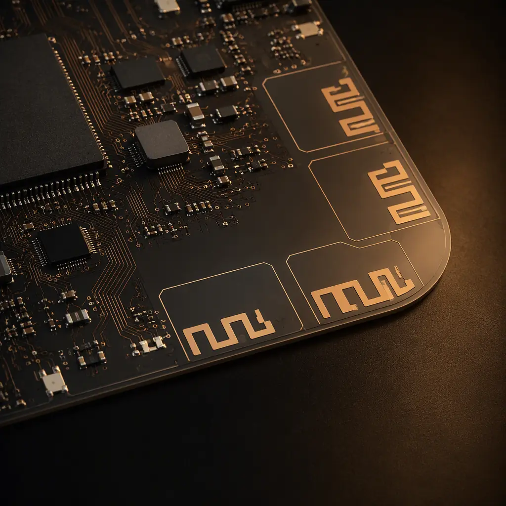
Respect the Antenna Keep-Out Zone
Antenna vendors specify a keep-out area — typically 3–5 mm around the antenna element with no copper, no components, and no traces. Violating it detunes the antenna and shifts the resonant frequency. Print the keep-out on the silkscreen and review it in DFM; it is the most common Wi-Fi layout defect we see in first-article reviews.
Separate Antennas by More Than the Minimum Distance
For spatial isolation, place antennas at opposite board edges where possible — aim for ≥ 20 mm separation between 2.4/5 GHz antennas and the 6 GHz antenna, and ≥ 15 mm between any antenna and the SoC. Isolation between the 5 GHz and 6 GHz radios matters most, because their bands are adjacent and the filters are not infinitely sharp.
Shield the Front End, Not Just the SoC
The RF front end (power amplifier, LNA, antenna switch) should sit under a shield can with a continuous fence and dense ground vias — same discipline as the GNSS case, but with more radios to isolate. Our EMC/EMI compliance guide covers shield design and emission control for multi-radio boards.
Assembly-Level RF: Solder Voids and Stencil Design
The RF performance designed into the layout can be destroyed at assembly. Three assembly details matter specifically at 6 GHz:
Control Solder Voids Under the PA and LNA
Power amplifiers rely on the ground pad and thermal vias for both heat and RF ground. Large solder voids under the exposed pad raise thermal resistance and add inductance — degraded output power and spurious emission risk. Specify X-ray inspection of the PA/LNA ground pads and keep voiding under 25% per IPC-A-610 class criteria. Our AOI/X-ray/SPI guide covers void acceptance practice.
Keep Solder Mask and Silkscreen Off RF Traces
Solder mask has its own Dk (3.2–4.0) and sitting directly on an RF trace changes its effective impedance — sometimes by several percent at 6 GHz. For critical RF traces, specify mask-defined openings (soldermask over bare copper with the trace exposed) or account for mask Dk in the impedance calculation. Never place silkscreen on an RF trace; its ink is lossy and its thickness is uncontrolled.
Design the Stencil for the Shield Cans and Fine-Pitch Parts
Wi-Fi boards mix large shield cans, fine-pitch RFICs, and small passives. The stencil must step up thickness for the cans without starving the 0201 pads — a stepped stencil or a second paste pass for cans is the standard solution. Review the stencil design with the fab; our stencil design guide has the aperture rules.
Certification: FCC, and SRRC for China-Bound Products
Most English-language guidance stops at FCC, but if your product ships to China — or is manufactured there — SRRC (State Radio Regulation Committee) approval is mandatory for devices with Wi-Fi transmitters. A few realities that affect the PCB design:
SRRC Covers the 6 GHz Band With Its Own Rules
China's SRRC regulates the 6 GHz band (5925–7125 MHz) with specific power limits and may require additional testing for Wi-Fi 7 devices. If you plan to sell in China, verify the current SRRC requirements early — a design that passes FCC may still need hardware changes (e.g., lower EIRP, different antenna gain) for SRRC.
Design for Certification Margin, Not the Limit
Every Wi-Fi device needs margin to its EIRP limit to survive unit-to-unit variation. A design that sits exactly at the limit in the lab will fail in production. Keep 2–3 dB of headroom, which usually means slightly lower PA output or a slightly less efficient antenna — decisions made in the RF budget, not discovered at the compliance lab.
Freeze the Layout Before Certification Testing
Certification results apply to the exact layout tested. Any change to antenna placement, stackup, or front-end routing after certification means retesting. Do the DFM review, first-article verification, and any impedance fixes before the compliance submission — our first-article inspection guide is the checklist to run first.
Summary: The Wi-Fi 7 Board Checklist
A Wi-Fi 7 board works when the RF chain is treated as a transmission-line problem from SoC to antenna: hybrid materials where the loss budget demands them, real measured impedance with documented tolerance, continuous return paths with no plane splits, back-drilled or avoided via stubs, respected antenna keep-outs, and assembly controls on voids and mask. None of this is exotic — it is disciplined RF layout plus a manufacturer that measures what it builds.
At Huaxing PCBA, we manufacture Wi-Fi 6E/7 boards up to 32 layers with low-loss hybrid laminates, ±5% impedance control, and back-drilling capability. Our DFM review checks antenna keep-out, plane continuity, via stub risk, and stencil design before tooling. Read our RF manufacturing guide to prepare your design, or send your files for a free DFM review and quote.
