

Most incoming-inspection disputes on a new board trace back to one misunderstanding. IPC-2221 is a design standard. IPC-6012 is an acceptance standard. A design can satisfy every limit in IPC-2221 and still be rejected at incoming inspection under IPC-6012 or IPC-A-610, because the two documents answer different questions: "what should the designer draw" versus "what will the customer accept on the delivered board." Design engineers who treat IPC-2221 tables as a checklist to just barely clear are the single most common source of first-article rejection and costly redesign cycles.
This guide covers what the standard's key tables actually specify, how to read them without misapplying the defaults, and — the part standards portals never publish — the three-column reality of standard minimum versus what a fabricator holds routinely versus what requires a premium process. Our facilities run 8 SMT lines with fabrication up to 32 layers out of Shenzhen, so the capability figures below are shop-floor numbers, not marketing claims.

What IPC-2221 Actually Governs (and What It Does Not)
IPC-2221 is the generic design standard for printed boards. It sets the rules you design to: conductor spacing versus voltage, conductor width versus current, hole size and annular ring relationships, and the mechanical and thermal ground rules. It does not tell you how much variation will be accepted on the finished board. That job belongs to a separate family of documents, and confusing the two is where most friction with a fabricator begins.
| Document | Role | Answers the question |
|---|---|---|
| IPC-2221 | Design standard | What spacing, width and hole geometry should be drawn |
| IPC-6012 | Acceptance (rigid boards) | What variation in the finished rigid board is acceptable |
| IPC-6013 | Acceptance (flex / rigid-flex) | Same, for flexible and rigid-flex constructions |
| IPC-A-610 | Acceptance (assembly) | What soldered assemblies look like when acceptable |
The practical consequence: a board drawn at exactly the standard minimum spacing, with the minimum annular ring, tightens the fabricator's process window to zero. Any etch variation, any drill registration drift, any plating thickness swing pushes the finished board outside IPC-6012 acceptance. The design is compliant. The build is not shippable in that form. That is a design margin problem, not a manufacturing failure.
The single most useful habit: when you read a number in IPC-2221, ask whether it is a minimum the design must not go below, or a nominal the design should aim at. The standard provides floors. It almost never provides targets. Your fab's process capability is the target.
Conductor Spacing vs Voltage — Reading the Table Correctly
The conductor spacing table is the most cited and most misapplied part of IPC-2221. It is organized by voltage bands (commonly presented as B1 through B4) and, critically, splits on three conditions that people routinely ignore: external versus internal conductors, coated versus uncoated surfaces, and altitude derating above sea level.
The internal-versus-external split matters because internal layers are laminated in resin with no air or surface contamination path, so they tolerate tighter spacing for the same voltage than an exposed external surface. The coated-versus-uncoated split matters even more in practice: a conformally coated assembly can often use spacing one band tighter than the same design left bare, which is why conformal coating is a legitimate spacing-margin tool and not just an environmental protection step.
Identify the working voltage, not the nominal rail
Spacing is set by the highest sustained potential difference between two adjacent conductors, including transients your circuit will actually see. A "48 V" design with a 120 V switching node ringing at start-up needs spacing for the transient, not the nominal. This is where engineers most often under-specify, and it is also where high-voltage designs diverge sharply from low-voltage practice.
Decide coated or uncoated before you pick the band
If the exposed side of the board will receive conformal coating, you can generally use the tighter spacing column for that surface. If any area stays bare — test points, connectors, exposed pads — that area is uncoated and must meet the wider requirement. Mixed assemblies need mixed rules on the same board.
Derate for altitude if your product flies or climbs
Paschen's law means breakdown voltage falls as air pressure drops. The standard's altitude derating factors apply to any product specified for high-altitude operation, aviation, or sealed enclosures that vent during thermal cycling. Products destined for satellite and LEO applications and aerospace work must account for this explicitly.
Remember the table's assumption about environment
The base spacing values assume a controlled environment. Condensation, conductive dust, flux residue and ionic contamination all reduce effective breakdown distance. Where the end product faces humidity or contamination, spacing should be widened beyond the table value or the surface properly cleaned to ionic standards and coated.
Trace Width vs Current — The Chart Everyone Misreads
The second most cited table is conductor width versus current, and it carries the same trap. The value you look up is valid only for the specific combination of copper thickness, layer position and permitted temperature rise. Two boards with identical trace widths can carry very different currents because those three variables differ.
The most consequential misunderstanding is the external-versus-internal gap. An external trace on an outer layer is cooled by convection and radiates to open air. An internal trace is laminated between dielectric layers, so heat has a much longer path to escape. As a rule of thumb, an internal layer trace needs roughly double the cross-sectional area of the external equivalent for the same temperature rise. Designers who copy an outer-layer width calculation onto an inner-layer plane and call the current rating identical are building in a thermal problem.
Copper thickness compounds this. Doubling from 1 oz to 2 oz does not just halve resistance — it changes the entire current-versus-rise curve, which is why heavy-copper constructions follow different rules again. If your design carries sustained current, work through the trace width and current capacity calculations per layer, not once for the board.
| Condition | Effect on required width | Where it bites |
|---|---|---|
| Internal layer vs external | ~2x cross-section for same rise | Power planes, inner-layer routing |
| 1 oz vs 2 oz copper | 2 oz roughly halves width for same current | High-current, motor drive, power supply |
| 10 °C vs 20 °C rise budget | Allowance widens substantially at 20 °C | Cost-sensitive consumer boards |
| Sustained vs transient current | Transients sized on thermal mass, not steady state | Inrush, motor start, capacitor charge |
Procurement tip: if your board has a heat-intensive region, ask your fab for the current-versus-temperature-rise assumption used in DFM. A fab that answers "internal layers, 10 °C rise, 1 oz" has actually checked it. A fab that answers "IPC-2221" has not.
Minimum Hole Size, Annular Ring and Aspect Ratio
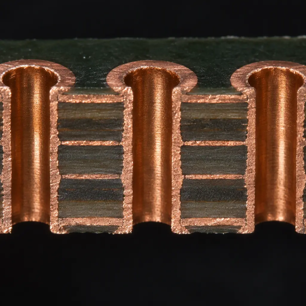
Hole geometry is where IPC-2221 interacts with manufacturing capability most directly, and where the standard's individual rules are often satisfied while the combination is not buildable. Three quantities are coupled: the finished hole diameter, the annular ring (the copper pad remaining around the hole), and the aspect ratio (board thickness divided by hole diameter).
IPC-2221 sets a minimum annular ring based on whether the hole is supported or unsupported and on the acceptance class of the product. What designers miss is that this ring is a finished-board minimum, not a drill offset allowance. Drill registration on a production panel is not perfect — the drill wanders relative to the pad artwork by a fraction of a millimetre, and that wander has to be absorbed by the ring. If you draw exactly the minimum ring, normal registration drift takes the finished board below the minimum, and the drill breakout is an acceptance failure even though the design was compliant on paper.
Size the ring to absorb registration, not to pass the drawing
A ring with no margin beyond the standard minimum is a design that assumes perfect registration. Production panels do not have perfect registration. Add allowance so normal drift still lands inside acceptable limits on the delivered board.
Check aspect ratio after you set the hole, not before
Aspect ratio is a consequence of hole diameter and board thickness. Choosing a small via to save routing space on a thick board can push you past practical plating depth limits, where achieving uniform copper through the barrel becomes slow, expensive, or unreliable. The relationship between drill diameter, thickness and plating reliability is covered in detail in our guide to via aspect ratio limits.
Do not mix hole classes casually in one design
A board with mechanical holes, component holes, standard vias and microvias asks the fab to hold several different tolerances at once, often with different drilling and plating sequences. Grouping similar hole sizes lets the fab run fewer drill hits and hold tighter control. Every distinct tooling step is a cost and a tolerance risk.
Confirm the acceptance class before you finalize tolerance
An IPC Class 3 board carries tighter annular ring and plating requirements than Class 2, and the same design may be compliant at one class and not the other. Decide the class early, because IPC Class 2 versus Class 3 differences ripple through ring, plating and inspection requirements.
Where the Standard's Minimums Stop Being Manufacturable
This is the section standards documents cannot give you, because it depends on process capability rather than on a specification. The table below separates three tiers: the floor the standard permits, what a competent fabricator holds routinely without special handling, and what is achievable but carries real cost and yield risk. Numbers are indicative of mainstream Shenzhen capability in volume production.
| Parameter | Standard floor | Routine production | Premium / risk |
|---|---|---|---|
| Min trace / space (1 oz outer) | Per IPC-2221 table by design rule | 0.10 mm / 0.10 mm | 0.075 mm / 0.075 mm |
| Min hole (mechanical drill) | Limited by plating capability | 0.20 mm | 0.15 mm |
| Min annular ring (finished) | Class-dependent minimum | +0.05 mm margin above floor | Requires HDI sequence |
| Max aspect ratio (standard plating) | Practically limited | 10:1 | 16:1 with controlled plating |
| Layer count | Application dependent | Up to 32 layers | Higher with special lamination |
| Min dielectric thickness | Material dependent | 0.075 mm | 0.05 mm |
The volume yield note matters more than the raw number. A 0.075 mm trace at a few hundred boards is a different proposition from the same trace at fifty thousand panels, because tight geometry amplifies every process variation into a yield loss. Designers should treat the premium column as a question to ask, not a target to design to by default.
Design reality check: the cheapest board is not the one designed at the smallest geometry the fab says it "can do." It is the one designed at the largest geometry that still meets the electrical and mechanical requirements. Tight geometry you do not need is money spent on yield risk.
IPC-2221 vs IPC-6012 — Design Intent vs Delivered Board
The hand-off between design and acceptance is the crux. IPC-2221 describes the board you intend to make. IPC-6012 describes the board you accept when it arrives. Conformance to the first says nothing directly about conformance to the second, because the second contains tolerances — on hole size, ring, plating, bow and twist, conductor width — that the finished board must meet within stated limits.
In practice this is where first-article inspection and new-product introduction live. A board designed right at the IPC-2221 floor will typically produce a first article that needs the fabricator's process centred very precisely to pass IPC-6012, and centring that tightly is expensive. A board designed with deliberate margin produces a first article that passes with the process running normally. The margin you build into the design is paid for once; the process control you need without it is paid for on every board.
Where new-product introductions go wrong most often is underestimating this. The NPI process exists to catch it before volume, and a shift-left DFM check should happen before the design freezes, not after the first panels are built.
Design Rules Checklist for Your Next RFQ
Use these eight points when preparing a request for quotation. They are the questions that most often determine whether a quote is accurate and a build is smooth.
State the acceptance class you need
Class 1, 2 or 3 changes what the fabricator must hold. Stating it up front avoids a quote built on the wrong tolerances.
Provide the highest working voltage between adjacent conductors
Not the nominal rail. This determines the spacing rule that applies, and it is frequently the item that pushes a design into a different band.
Specify the copper weights per layer
Mixed copper weights across layers are normal in power designs and must be quoted per layer, not as a single board figure.
List your minimum geometry and mark it as a requirement or a preference
A minimum you can relax is a cost lever. A minimum you cannot relax is a constraint. Fabs quote differently depending on which it is.
Note the operating environment
Altitude, humidity, condensing atmospheres and contamination all change spacing requirements. Stating the environment lets the fab flag margin issues before production.
Confirm maximum aspect ratio is within process capability
Provide finished board thickness and minimum via diameter so the aspect ratio is explicit rather than discovered during DFM.
Ask which IPC-2221 assumptions the DFM check used
The answer tells you whether a real check was run. See our guide to shift-left DFM verification for what a substantive check should contain.
Require the acceptance standard in writing
State IPC-6012 with the class, and IPC-A-610 for assembly acceptance. Naming the standards removes ambiguity before the first article, not after.
Summary and Next Steps
IPC-2221 tells you the floor, not the target. The three conditions that decide whether your design is actually buildable are the ones the tables split on and engineers most often skip: external versus internal, coated versus uncoated, and design-class versus acceptance-class. Get those right and the geometry questions answer themselves with margin instead of guesswork.
At Huaxing PCBA we run design-rule checks against our actual process capability, not against a generic table, and we will tell you which of your minimums are costing you yield and which are free. Our facilities hold IATF 16949 and ISO 9001 certification with fabrication to 32 layers and 8 SMT lines. Read our trace width and current capacity guide or send your Gerber and stackup for a free DFM review — quote in 24 hours.
