
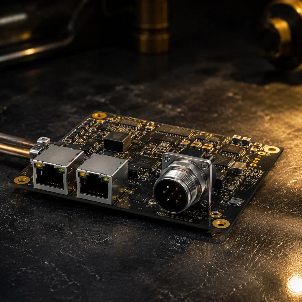
Industrial Ethernet, EtherCAT, PROFINET, EtherNet/IP, POWERLINK, is the backbone of modern factory automation, and almost all of it runs on 100BASE-TX physical layers. The protocol sits in software, but the physical layer lives on your PCB, and the factory floor is a hostile environment for it: motor drives and welding robots radiate noise, long cable runs pick up surges, and enclosures with poor grounding push transients into the port. A control board that passes a bench test but resets every time a servo starts is a classic sign that the Ethernet PHY section was designed like an office NIC.
This guide covers the layout and protection rules that make industrial Ethernet ports reliable: PHY and magnetics placement, 100 Ω differential routing, ESD and surge protection per IEC 61000-4-2/-4-4/-4-5, galvanic isolation, and the PCB stackup decisions that keep emissions in check. Huaxing PCBA builds PLCs, servo drives, HMI panels and IoT gateways for automation customers across 30+ countries. These are the rules our DFM team checks on every industrial Ethernet board.
Why Industrial Ethernet Is Different From Office Ethernet
Before touching the layout, it helps to understand the three differences that change PCB design decisions:
Real-time determinism at 100 Mbps
EtherCAT passes process data through each slave node in hardware with submicrosecond jitter, and PROFINET IRT does the same with time slicing. The PHY and magnetics must deliver clean signal edges at 100BASE-TX signaling rates (125 MBaud MLT-3) because bit errors mean missed cycle deadlines, not just retries. There is no retry in real-time operation, a corrupted frame is a lost cycle.
Extended temperature and vibration
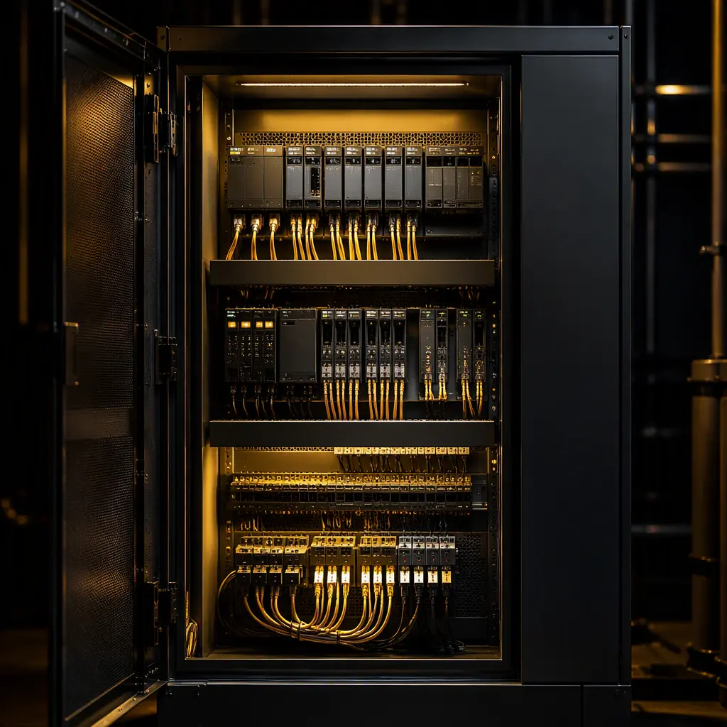
Industrial boards are rated for -40 °C to +85 °C ambient, often with conformal coating and vibration testing to IEC 60068-2-6. The PHY, magnetics and connector choices must be industrial-grade parts with full temperature ratings. Commercial silicon that works at 25 °C in a lab can fail intermittently at 70 °C inside a control cabinet next to a VFD.
EMC requirements an office NIC never faces
Industrial equipment is tested to IEC 61000-4-2 (ESD, ±8 kV contact), IEC 61000-4-4 (EFT, ±2 kV), IEC 61000-4-5 (surge, ±1 kV line-to-line), and radiated immunity IEC 61000-4-3 at 10 V/m. These tests inject energy directly into the Ethernet port, which is why the port needs protection components and layout discipline, the topic of our PCB EMC compliance guide applied at the port level.
Key Takeaway: Industrial Ethernet design is 80% about the physical layer: protection, isolation, impedance and grounding. Protocol compliance is a firmware concern; field reliability is a PCB concern.
PHY, Magnetics and Connector Placement
The PHY-to-connector path is a tightly coupled analog chain. Its layout rules are non-negotiable:
Keep the PHY-to-magnetics-to-connector path short
The total trace length from PHY TX/RX pins to the connector should be under 25 mm where possible. Every millimeter of unshielded trace is an antenna for both emissions and immunity. Place the magnetics (or the integrated-connector module) immediately beside the PHY, and never route the MDI side (the cable side of the magnetics) across the board or near other noisy traces.
Choose integrated magnetics or separate modules deliberately
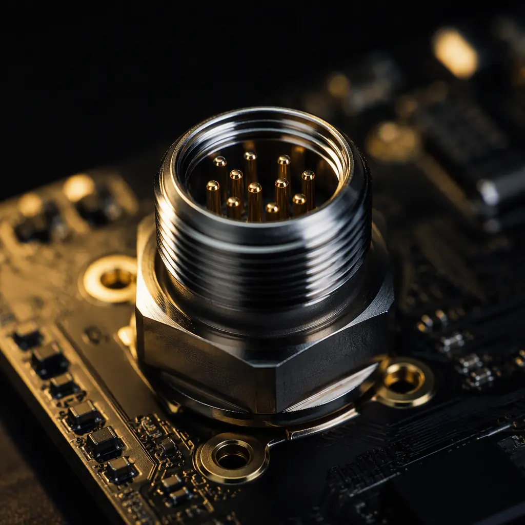
Industrial boards use either RJ45 jacks with integrated magnetics or discrete magnetics plus a separate connector (often M12 for IP67 field wiring). Integrated jacks save space but fix the transformer vendor; discrete magnetics let you select industrial-rated transformers with higher isolation (1.5 kV RMS minimum, 2.25 kV preferred for surge-heavy environments). For EtherCAT nodes, the connector and PHY selection must also respect the EtherCAT Technology Group's compliance requirements.
Bob Smith termination on the MDI side
Terminate the four unused MDI pairs with the classic Bob Smith network, a 75 Ω resistor from each pair center to a common node with a 1 nF/2 kV capacitor to chassis ground (or protective earth). This gives a controlled AC path for common-mode noise and is one of the cheapest EMC wins on an Ethernet port. The capacitor's voltage rating must survive the surge test, not just the working voltage.
Chassis ground plane under the connector
Route the shield of the RJ45 or M12 connector to a chassis ground plane (not the logic ground) with a solid, low-inductance connection. The magnetics' isolation barrier should straddle the boundary between logic ground and chassis ground. This is the same grounding discipline covered in our Ethernet PHY layout guide, applied with industrial surge ratings.
100 Ω Differential Routing and Stackup
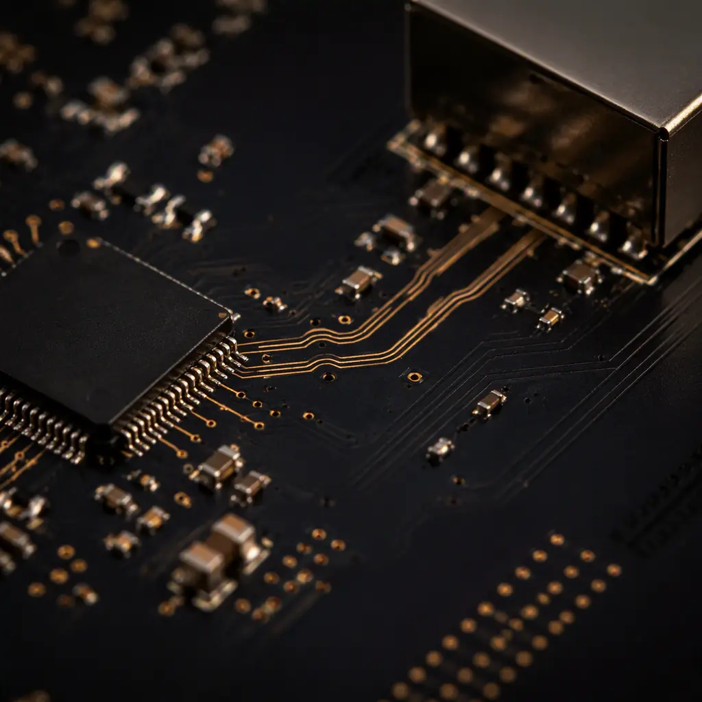
The TX+/- and RX+/- pairs must be routed as controlled-impedance differential pairs:
100 Ω differential, ±10%, referenced to a solid plane
100BASE-TX requires 100 Ω differential impedance with a typical tolerance of ±10% (stricter for some PHY vendors). The pairs must reference an uninterrupted ground plane, a split plane under the PHY section destroys impedance control and adds common-mode noise. Our impedance control guide explains how stackup and trace geometry interact, and the stackup guide covers plane assignment.
Match pair lengths and keep pairs together
Keep the two traces of each pair matched within 5 mm (ideally 2 mm) and route them together without separating them around vias or components. Avoid crossing a split in the reference plane; if a via transition is unavoidable, place ground vias adjacent to the signal vias to maintain a return path.
Keep high-speed digital noise off the PHY section
The PHY's digital side (MII/RMII/RGMII buses, clock, reset) must be routed away from the analog MDI section. Do not run the RMII clock or SPI buses parallel to the differential pairs. A ground guard trace between the digital and analog PHY sections helps in dense layouts.
Decouple the PHY power rail properly
PHYs are sensitive to supply noise on their analog rails (AVDD). Use a ferrite bead plus a 10 µF bulk and 100 nF/1 nF MLCCs close to the PHY pins, and give the PHY its own power plane island if the board has multiple 3.3 V consumers. A noisy PHY supply shows up directly as jitter on the MDI signal.
ESD, Surge and Transient Protection for the Fieldbus Port
This is the section that separates industrial boards from office boards. The port must survive:
| Test (IEC 61000-4-x) | Typical Industrial Level | Port Protection |
|---|---|---|
| ESD 61000-4-2 | ±8 kV contact / ±15 kV air | TVS diode array on MDI, spark-gap pad under connector |
| EFT 61000-4-4 | ±2 kV, 5/50 ns | Common-mode choke + TVS, ferrite on cable shield |
| Surge 61000-4-5 | ±1 kV line-line / ±2 kV line-earth | TVS with ≥ 1.5 kW peak pulse power, series resistors |
| Radiated immunity 61000-4-3 | 10 V/m, 80 MHz–6 GHz | Shielded connector, chassis ground continuity |
Place TVS diodes as close to the connector as possible
TVS clamping performance depends on lead inductance, a TVS 10 mm away from the connector clamps several hundred volts higher than one at 2 mm. Put the protection array directly behind the connector, before the magnetics, so the transformer never sees the full transient. For EFT and surge, a common-mode choke between connector and magnetics is standard practice on industrial designs.
Spark-gap pad under the connector
Many industrial Ethernet boards add a bare-copper spark gap pad under the RJ45 or M12 footprint to chassis ground. It provides a controlled discharge path for extreme ESD events that exceed the TVS rating, an inexpensive insurance layer that EMC labs recognize.
Galvanic isolation for long runs and mixed grounds
When nodes are powered from different supplies (separate 24 V domains) or the cable runs between buildings, use an isolated PHY or an isolation transformer plus isolated power (e.g., a small DC-DC or a transformer driver like the NVE IL4xxx family). Isolation breaks ground loops that otherwise cause random resets and communication errors. The isolation barrier placement on the PCB must keep creepage/clearance per IEC 60601-style rules, see our high-voltage design guide for barrier layout.
EMC and Shielding Around the Port
Fieldbus ports are both the most sensitive and the most radiating part of an industrial board:
Keep the MDI section off the board edge
Traces between the magnetics and connector should never run parallel to the board edge, edge-coupled noise radiates efficiently. Keep the PHY/magnetics/connector cluster in one corner with a clear keep-out zone on the inner side.
Via stitching around the port area
Stitch ground vias every 2–3 mm around the PHY section and connector footprint to tie top and bottom ground planes together, reducing the common-mode loop that radiates. This is cheap and one of the most effective emissions fixes.
Conformal coating for condensation environments
Control cabinets in food, beverage or high-humidity plants get condensation on boards. A 25–75 µm acrylic coating over the PHY and protection section prevents leakage paths that degrade the port's immunity margin. Our conformal coating guide covers material selection for industrial environments.
Design Review Checklist Before You Send Files to the Factory
Run this checklist before sending your industrial Ethernet board to production:
100 Ω differential impedance specified in the stackup
The fabrication notes must state 100 Ω ±10% differential for the MDI pairs, with the stackup designed to achieve it. Our manufacturing tolerances guide covers what tight-impedance control actually costs.
Test points for the PHY signals
Add test points on the RMII/MII lines and the MDI pairs for factory functional test, this is part of design for testability and lets your CM verify the port before the board is assembled into the machine.
Confirm the EMC test plan with your lab early
Pre-compliance EMC testing of the first prototype catches layout issues before tooling for production. A first-article with pre-compliance ESD and EFT testing costs a fraction of a redesign after field failures. See our testing methods guide for the full test portfolio.
Summary: Build the Port for the Floor, Not the Bench
Industrial Ethernet reliability is decided by a short list of physical-layer decisions: short PHY-to-connector paths, controlled 100 Ω routing over solid planes, TVS and common-mode protection sized for IEC 61000-4-x tests, chassis-ground discipline at the connector, and optional galvanic isolation for mixed-supply plants. Get those right and the protocol stack does its job; get them wrong and no amount of firmware tuning will fix intermittent resets.
At Huaxing PCBA, we manufacture and assemble industrial control boards, PLCs, servo drives, HMIs and gateways, with 2–32 layer capability, controlled impedance to ±5%, and in-house AOI, X-ray, ICT and functional test including Ethernet loopback testing. Send us your design and our DFM team will check the PHY section layout, protection placement and impedance requirements before production. Contact our engineering team or upload your Gerber files for a quote within 24 hours.
