
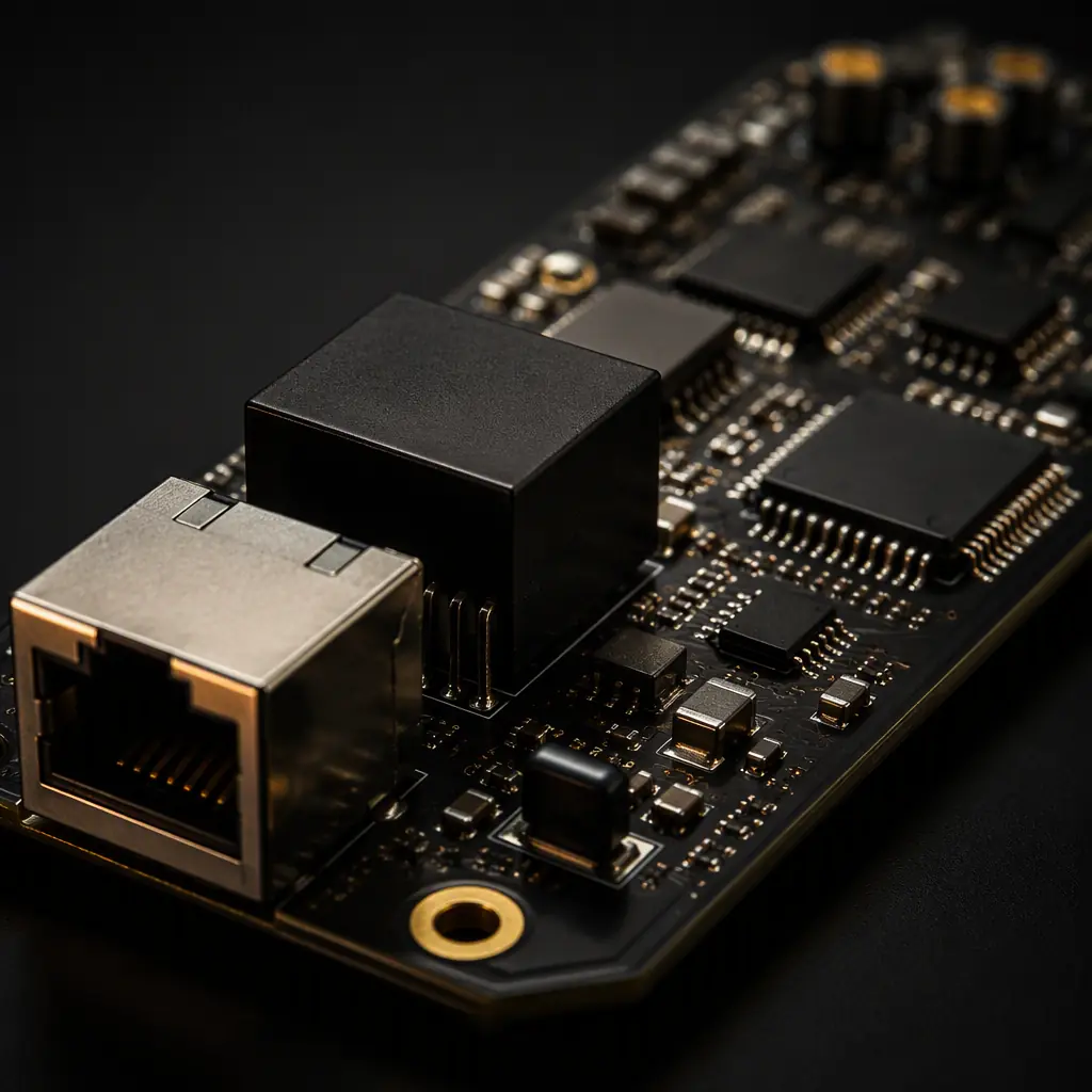
Ethernet is the default connectivity backbone of industrial IoT: gateways, PLCs, drives, and edge computers all speak 10/100/1000BASE-T over a cheap, unshielded twisted-pair cable that can run 100 meters and survive decades of industrial noise. The protocol's autonegotiation and error correction absorb a lot of sloppy layout — which is exactly why marginal designs pass the bench test and then fail in the field: link drops at temperature, intermittent CRC errors, or a radiated-emissions failure at the EMC lab.
Huaxing PCBA manufactures Ethernet-enabled boards for industrial automation, building automation, and IoT customers — up to 32 layers, controlled impedance to ±5% with coupon testing, 3/3 mil routing, and 8 SMT lines with full functional test support including live Ethernet link testing. This guide covers PHY placement, the magnetics rules that most layout engineers get wrong, 100 Ω MDI routing, the crystal and power sections, ESD protection, and the fabrication notes that make a Gigabit link reproducible across production.
Why the Magnetics Decide Link Quality
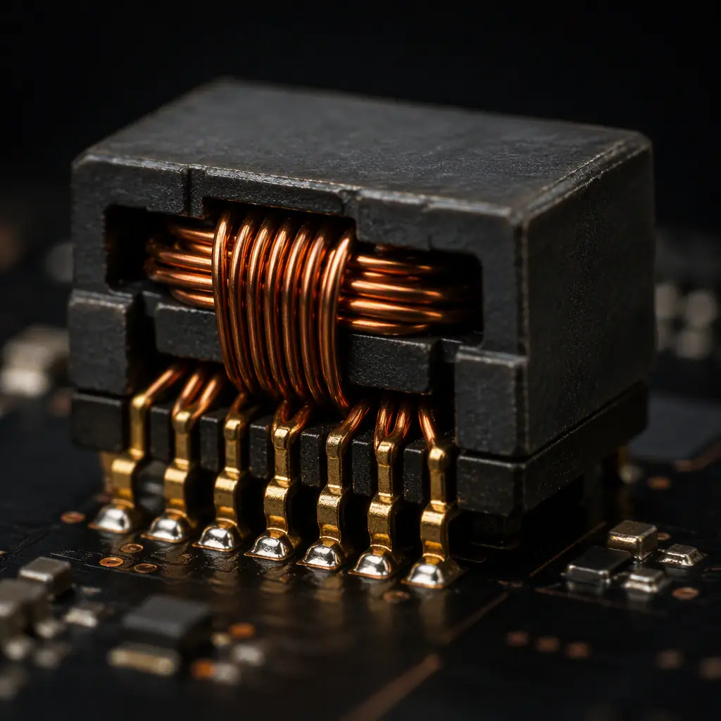
The Ethernet magnetics — the transformer module between the RJ45 jack and the PHY — do three jobs: they provide galvanic isolation (1.5 kVrms per IEEE 802.3), they reject common-mode noise from the cable, and they shape the signal through center-tap terminations. The magnetics are the most layout-sensitive component on the board, and most Ethernet field failures trace back to how they are placed and grounded. Our signal integrity guide covers the general high-speed rules; here are the Ethernet-specific ones.
Place the Magnetics Within 10-15 mm of the RJ45 Jack
The MDI traces between the connector and the magnetics are exposed to the outside world and act as antennas if they run too far. Keep this section as short as possible — under 15 mm is the common reference-design rule. If the board uses a jack with integrated magnetics, the rule moves inside the connector and your job is to route the PHY-side traces cleanly and provide the correct center-tap supply.
No Traces, No Copper, No Vias Under the Magnetics
The area directly under the magnetics module must be cleared of copper on all layers — no ground pour, no signal traces, no vias. The transformer couples energy between its windings and to the board; copper underneath creates an unintentional antenna and couples noise into the PHY. Reference designs typically specify a keep-out of 2-3 mm beyond the module footprint on every layer, with the ground pour resumed outside that zone and stitched with vias.
Use Bob Smith Termination and the Correct Center-Tap Supply
The classic Bob Smith termination — 75 Ω resistors from each MDI line to a common point, with a 1 nF/2 kV capacitor to chassis ground — provides a return path for common-mode energy and is required for passing radiated-emissions tests on unshielded twisted-pair designs. The transformer center taps go to the PHY's VDD (typically 3.3 V) through a decoupling capacitor for 100BASE-TX, or to a resistor network that biases the transmit pairs for 1000BASE-T. Follow the PHY datasheet's center-tap schematic exactly — getting this wrong produces a board that links but fails emissions testing.
Key Takeaway: The magnetics are a noise-isolation component, not just a connector accessory. Short MDI traces, a clean keep-out under the module, and the exact center-tap termination from the datasheet are the three rules that separate passing and failing EMC results.
MDI Differential Pairs: 100 Ohm Routing That Stays Tight
Each 1000BASE-T link uses four differential pairs (BI_DA through BI_DD), each running at 125 MBaud with PAM-5 modulation — a demanding signal by any standard. 100BASE-TX uses two pairs at 125 MBaud MLT-3. Both need controlled 100 Ω differential impedance and disciplined routing.
Route All MDI Pairs as 100 Ω Differential With Tight Coupling
Specify 100 Ω differential impedance ±10% (or tighter, ±5% for Gigabit) and route the pairs edge-coupled over a continuous ground plane. On a standard 1.6 mm FR-4 stackup, this works out to roughly 0.2 mm traces with 0.15-0.2 mm spacing on an outer layer. Keep intra-pair spacing constant for the entire route — every variation changes the impedance and creates a reflection point. Huaxing's impedance control to ±5% with TDR coupon testing makes Gigabit links reproducible across panels.
Match Pair Lengths Within 50 mil (1.27 mm) and Keep Inter-Pair Skew Under 0.5 ns
Gigabit Ethernet is extremely sensitive to skew: the four pairs must arrive at the receiver within tight timing windows. Length-match the two traces within each pair to within 50 mil, and match the overall lengths of the four pairs to within about 200 mil. Routing all four pairs on the same layer with the same number of vias keeps the delay uniform — avoid routing one pair on layer 2 and another on layer 4 with a different via count.
Minimize Vias; When Used, Keep Them Symmetric
Each via adds inductance and a small impedance discontinuity. Prefer routing the MDI section on a single layer; if a via pair is unavoidable, place the vias for both legs side by side and keep their stubs short by routing on adjacent layers. Vias in the MDI path are one of the first things an EMC consultant will question.
Keep Other Signals 5x the Pair Spacing Away
Aggressive signals — clocks, switching regulators, and the PHY's own MII/RMII/RGMII bus — must stay well clear of the MDI pairs. A spacing of at least 5 times the intra-pair spacing (roughly 1 mm) between an MDI pair and any other trace prevents crosstalk that degrades the eye diagram. Crossing other signals at 90 degrees is acceptable; running parallel is not.
| Parameter | 100BASE-TX | 1000BASE-T |
|---|---|---|
| Pairs used | 2 (TX, RX) | 4 (BI_DA - BI_DD) |
| Line rate | 125 MBaud MLT-3 | 125 MBaud PAM-5 |
| Differential impedance | 100 Ω ±10% | 100 Ω ±10% |
| Intra-pair length match | ≤ 50 mil recommended | ≤ 50 mil recommended |
| Isolation requirement | 1.5 kVrms | 1.5 kVrms |
| Max cable length | 100 m | 100 m |
PHY Placement, Crystal and Power Integrity
The PHY itself (parts like the TI DP83822, Microchip LAN8720A, Realtek RTL8211F, or Broadcom BCM54210) has modest layout demands compared with the magnetics — but three details consistently bite.
Place the PHY Close to the Magnetics, Not to the MAC
The MDI side of the PHY faces the magnetics and must stay short; the MAC side (MII/RMII/RGMII) is a parallel digital bus that tolerates longer traces. Position the PHY so the MDI pairs to the magnetics are the shortest routes on the board, even if that pushes the RGMII bus a little further. The RGMII bus at 125 MHz still needs length matching, but it is far more forgiving than the analog MDI side.
Crystal First, Then Decoupling, Then the Rest
The PHY reference clock (typically 25 MHz for Gigabit, or a 50 MHz oscillator) drives the transmit clock recovery, so its layout is part of signal integrity: place the crystal within 5 mm of the PHY's XI/XO pins, keep the traces short and equal, and never route the crystal traces under other components. Add 0.1 µF decoupling on every PHY supply pin with vias directly to the ground plane, plus a 10 µF bulk capacitor per supply rail. A noisy PHY supply shows up as jitter — and jitter shows up as intermittent link flaps.
Give the PHY Its Own Supply Section, Isolated From Switching Regulators
If the board has a DC-DC converter (and most industrial boards do — see our SMPS layout guide), keep the PHY's analog supply away from the switch node. A ferrite bead plus 10 µF/0.1 µF filtering on the PHY rail, and a ground pour that connects the PHY's ground pin to the plane with at least two vias, keeps switching noise out of the link. For PoE designs, the PHY supply section also interacts with the PSE/PD negotiation — our PoE design guide covers that in detail.
ESD, Surge and Industrial Transient Protection
An RJ45 connector is an open door for electrostatic discharge and, in industrial environments, surge events from long cable runs. IEEE 802.3 defines the isolation, but protecting the PHY beyond the magnetics is a board design decision.
Add a TVS Array at the Connector, Before the Magnetics
A low-capacitance Ethernet TVS array (parts like the SLVU2.8-4 or ESD7484, with under 1 pF per line to preserve signal quality) clamps ESD at the jack. Place it within 5 mm of the RJ45, with its ground connection straight to the chassis-ground zone. The TVS protects the magnetics and PHY from the 8 kV contact discharges that IEC 61000-4-2 testing applies directly to the connector shell and pins.
Connect the Connector Shell to Chassis Ground Through a Resistor-Capacitor Network
The RJ45 shield should not connect directly to the signal ground plane — that turns the cable shield into a noise antenna and can create ground loops between devices. The standard industrial approach is a 1 MΩ resistor in parallel with a 1-10 nF/2 kV capacitor from the shell to chassis ground, keeping the shield at a defined potential while blocking DC ground loops. If the design uses a metal panel, bond the chassis ground zone to the panel at a single point.
For Outdoor or Long-Run Links, Add Surge Protection
Industrial Ethernet ports that leave the enclosure (or run between buildings) need surge protection beyond ESD diodes — a GDT or TVS with higher energy rating on the magnetics' cable side, coordinated with the isolation rating of the transformer. This is a different protection tier from indoor ESD and should be specified with the project's immunity standard (IEC 61000-4-5 surge, level 2-4).
Putting It Together: A Gateway Board Layout Order
Industrial IoT gateways combine Ethernet with a host processor, memory, and fieldbus interfaces — our IoT PCB design guide and building automation guide cover the system-level picture. The Ethernet portion of the layout, in order:
Position the RJ45 Jack First, at the Board Edge
The jack defines the mechanical envelope (panel cutout, height, shielding). Place it at the edge with the chassis-ground zone around it, isolated from the signal ground by the RC network.
Then the Magnetics, Then the PHY, Then the MAC Interface
Work outward from the jack: TVS, magnetics with a clear keep-out underneath, PHY within a few millimeters of the magnetics, then the RGMII/MII bus to the processor. Lock these positions before routing anything else — the Ethernet section is the least flexible part of the board.
Route the MDI Pairs, Then the MAC Bus, Then the Power
MDI pairs first (short, 100 Ω, length-matched), then the parallel MAC interface with its own length matching, then the PHY power with ferrite filtering. Leave the magnetics keep-out untouched until the board is fully routed.


Manufacturing Notes for a Reproducible Ethernet Board
Ethernet performance depends on manufacturing consistency more than most board types — a 5% impedance drift changes the eye diagram, and inconsistent stackup ruins Gigabit links. Specify these on the fabrication drawing:
Impedance Coupons and TDR Report on Every Panel
Require 100 Ω differential coupons per layer and a TDR report with the shipment. Huaxing tests impedance to ±5% and provides the report automatically.
Controlled Dielectric and Stackup
Specify the dielectric material (e.g., FR-4 with controlled DK of 4.2-4.5 at 1 GHz) and the exact stackup — the impedance of the MDI pairs is set by the layer structure, so any substitution changes the link margin. If the board also carries high-speed signals elsewhere, our stackup design guide is the reference.
Functional Test: Live Link Test on Every Unit
Beyond AOI and ICT, Ethernet boards deserve a functional test that establishes a live link — at 1000BASE-T where applicable — and checks link status plus a packet loopback. A link test catches magnetics soldering defects, missing center-tap parts, and assembly issues that AOI cannot see.
Summary: The Ethernet Board Checklist
A production-ready Ethernet board has the magnetics within 15 mm of the jack with a clean keep-out underneath, Bob Smith termination and the datasheet center-tap network, four tightly coupled 100 Ω differential pairs length-matched within 50 mil, a PHY placed for short MDI routes with its crystal and decoupling in order, TVS at the connector, the shell grounded through an RC network, and a fabrication drawing that pins down impedance, dielectric, and stackup. When all of that is right, the link holds at temperature, passes emissions, and runs for a decade — which is exactly what industrial equipment buyers expect.
At Huaxing PCBA we manufacture Ethernet gateway, switch, and IoT boards up to 32 layers with impedance control to ±5%, 3/3 mil routing, and full assembly support across 8 SMT lines — including X-ray, conformal coating, and live Gigabit link functional testing. Our DFM review checks your magnetics placement, keep-outs, impedance requirements, and assembly notes before tooling. Read our switch and router PCB guide for the 100G/400G high-speed side of networking, or send your files for a free DFM review and quote.
