
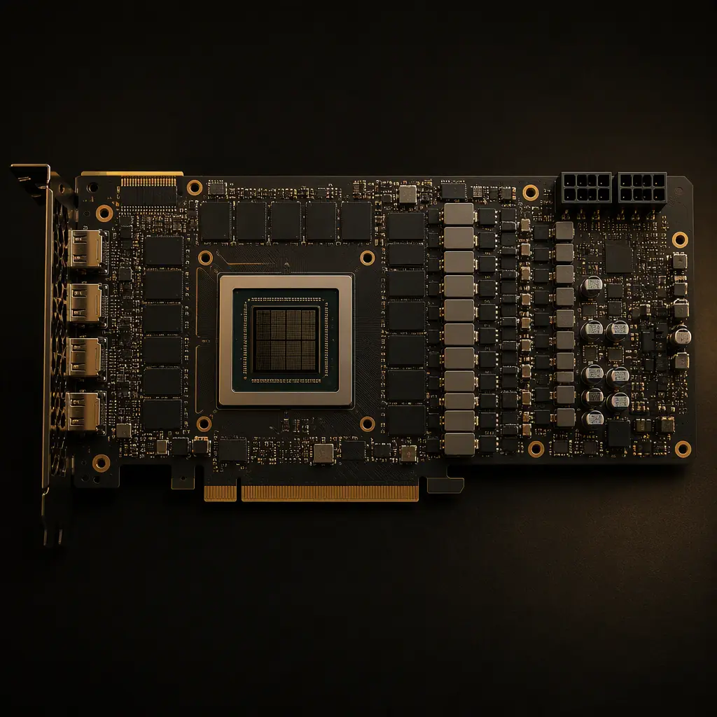
A modern graphics card is one of the most demanding PCBs in volume production. The GPU die itself is a 500–800 mm² silicon package with tens of thousands of bumps, surrounded by high-speed memory running at 21 Gbps per pin, and powered by a multi-phase VRM that must deliver hundreds of amps with ripple below 10 mV. Every one of those requirements lands on the PCB. And the board is where most graphics card projects either hit their performance target or get stuck in re-spin.
Huaxing PCBA fabricates GPU-class boards up to 32 layers with any-layer HDI and 3/3 mil trace/space, and assembles them across 8 SMT lines with 0.3 mm pitch BGA capability. This guide walks through the stackup, routing, power and thermal decisions that separate a reference design from a manufacturable product, and the DFM rules that keep 16-layer boards profitable at volume.
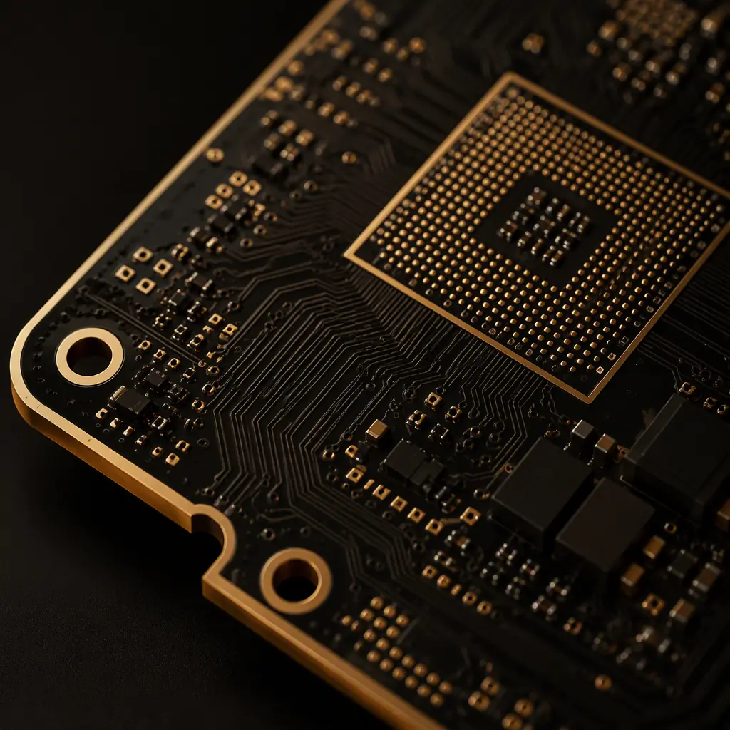
Why GPU Boards Are Different: Layer Count and Density
A GPU board is not a scaled-up motherboard. Three forces push the layer count up: the sheer number of signals escaping a 5,000+ ball BGA, the impedance-controlled routing required at PCIe 5.0/6.0 speeds, and the need for multiple solid reference planes under every high-speed group.
| Board Type | Typical Layers | Min Trace/Space | High-Speed Interface |
|---|---|---|---|
| Mainstream GPU (mid-range) | 10–12 | 3.5/3.5 mil | PCIe 4.0 |
| Enthusiast GPU (high-end) | 14–16 | 3/3 mil | PCIe 5.0 + GDDR6X |
| AI accelerator / workstation | 16–20+ | 3/3 mil, HDI microvias | PCIe 5.0/6.0 + HBM |
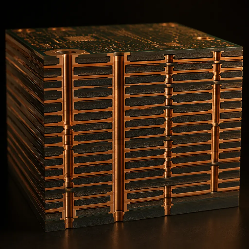
Above 12 layers, blind and buried vias stop being optional. A 16-layer board with only through-hole vias cannot escape a dense BGA fanout without excessive via counts and routing congestion; HDI microvias (laser-drilled at 0.075 mm) free up the escape channels. Our HDI technology guide covers the via structures, and PCB stackup design walks through layer assignment for mixed high-speed and power boards.
Key Takeaway: Layer count is a signal-integrity decision before it is a cost decision. If your design needs 16 layers for routing, dropping to 12 to save money will cost more in re-spins than it saves in fabrication.
Stackup Architecture: Reference Planes and Material Selection
The stackup of a GPU board has one job: give every high-speed group an unbroken reference plane directly beneath it. For PCIe 5.0 at 32 GT/s, the return-current path must be a solid copper plane, not a fragmented power island.
Signal-adjacent plane discipline
Every differential pair layer sits between two solid planes: typically ground above and below, with the dielectric thickness tuned for the target impedance. For 85 Ω differential (PCIe) and 40 Ω single-ended (memory), the layer spacing is controlled to ±5%, which is why GPU boards are quoted as impedance-controlled jobs with coupon testing on every panel. Our impedance control guide explains the tolerance chain from stackup to final test.
Low-loss laminate where the speed demands it
Standard FR-4 works for PCIe 4.0 (16 GT/s) on short traces. Once you cross into PCIe 5.0 (32 GT/s) or GDDR6X at 21 Gbps, the loss budget forces a mid-loss or low-loss laminate on the high-speed layers. Materials with a dissipation factor around 0.004–0.010 at 1 GHz rather than the 0.020 of standard FR-4. The rest of the board can stay on FR-4 to control cost. Material selection logic is in our PCB materials guide and laminate selection guide.
Power planes sized for hundreds of amps
The GPU core rail at 0.9–1.1 V carries 300–500 A in flagship cards. That current needs multiple dedicated power planes and, in many designs, an internal copper pour that spans nearly the full board width. Voltage drop across the plane is the reason flagship cards use 8-layer-plus power sections: the IR drop between the VRM output and the die must stay under about 20 mV at full load. Power-plane and decoupling strategy is covered in detail in our power integrity design guide.
Routing GDDR6X and PCIe: What 21 Gbps Does to Layout Rules
High-speed memory routing on a GPU board is the tightest routing discipline in consumer electronics. GDDR6X uses PAM4 signaling at 21 Gbps per pin, effectively 10.5 Gbps of data per symbol, which halves the margin available to impedance mismatch, crosstalk and via stubs.
Length-matched groups, not individual nets
Memory controllers route in byte lanes: 8 data bits plus DQS must be length-matched within roughly ±1.5 mm, while the entire channel stays within a few millimetres of the controller's target. Modern layout tools handle this automatically, but the PCB manufacturer must honour the specified tolerance. At 21 Gbps, a 5 mm skew is a real timing error. Our DDR4/DDR5 routing guide covers the same discipline for system memory.
Via stubs are the enemy at 32 GT/s
PCIe 5.0 traces that change layers through a through-hole via leave a stub, the unused portion of the barrel, that rings at multi-gigahertz frequencies and eats the eye diagram. Backdrilling removes the stub from the non-connection side; on high-speed signal layers it is effectively mandatory above 25 GT/s. Backdrill depth tolerance and design rules are detailed in our PCB backdrilling guide.
Crosstalk budgets between byte lanes
At 21 Gbps, even adjacent-layer coupling becomes measurable. Routing rules call for 3× dielectric-height spacing between differential pairs, guard vias at layer transitions, and never routing two byte lanes directly over each other on adjacent layers. Our crosstalk analysis guide and signal integrity overview give the quantitative rules.
VRM Layout: Delivering 450 W Without Voltage Droop
The power stage of a flagship GPU is a 12–20 phase buck converter that must hold the core rail within a few percent while load steps of 100+ A occur in microseconds. Layout decides whether that is achievable.
Phase cells placed tight to the GPU package
Each phase, driver, MOSFET pair and inductor, forms a loop that must be physically small to limit parasitic inductance. The phase cells ring the GPU package on all four sides, with the output inductors within a few millimetres of the BGA's power bumps. Trace width and copper weight follow the current: the high-current output traces need 2–4 oz copper on the outer layers. Our trace width vs current capacity guide has the sizing tables.
Decoupling: bulk on the back, ceramic under the package
Bulk capacitance (polymer and tantalum) sits on the back side of the board opposite the VRM; 0402 and 0201 ceramic capacitors fill the keep-out zones directly under the GPU socket area on the top side, within 1–2 mm of the power pins. The via count between the capacitor pads and the power plane is part of the design, 0.3 mm vias on 0.5 mm pitch under each decoupling site. This is the same philosophy, at higher density, as our power integrity guide describes for general boards.
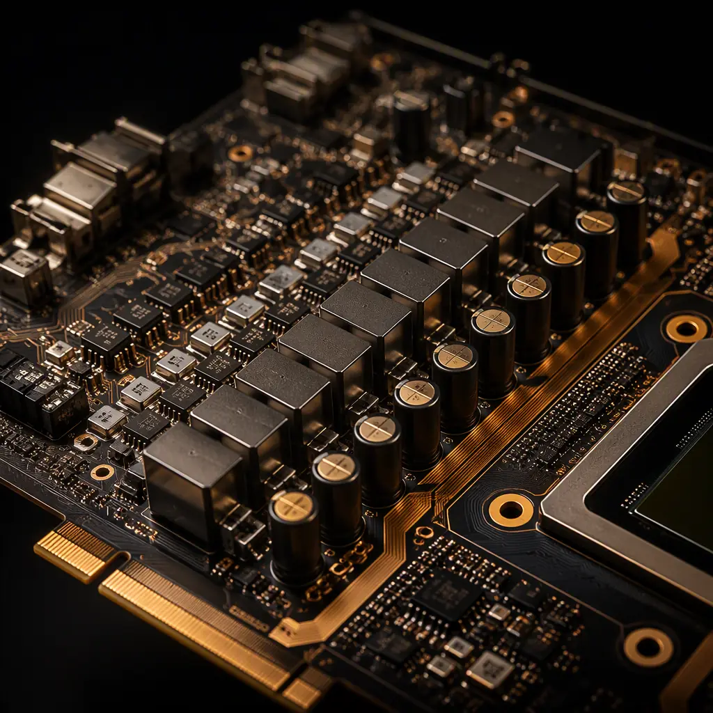
Reliability Reality: The first thing a graphics card board fails on is not the GPU silicon. It is the VRM: MOSFETs starved of copper, inductor pads with insufficient via stitching, or decoupling placed too far from the load. The power section deserves as much layout effort as the high-speed section.
Thermal Management: Moving 450 W Out of a 250 W Slot Envelope
A flagship GPU dissipates 350–450 W into a dual-slot heatsink. The PCB is the middle layer of that thermal path: heat flows from the die into the package, through BGA solder balls, into the board's copper planes, and down to the backside plate and heatsink.
Thermal vias under the die and VRM pads
Directly under the GPU package, arrays of 0.25–0.3 mm thermal vias conduct heat into the internal planes and down to the backside heatsink plate. A flagship card carries several thousand thermal vias. The same pattern repeats under every VRM MOSFET and inductor. Via-array sizing and plane conduction are covered in our PCB thermal management guide.
Backside copper pour for the cooling plate
Many flagship cards use a backplate that doubles as a heat sink. The backside of the PCB gets a continuous copper pour (1–2 oz) with solder mask openings where the plate mounts, so the metal-to-copper interface conducts rather than insulates. Differential expansion between the thick copper and the laminate needs the same CTE management our warpage prevention guide describes. GPU boards are among the worst warpage offenders at reflow temperature because of their asymmetric copper distribution.
Component derating in the hot zone
VRM components operate 20–40°C above ambient inside a gaming chassis. Inductor saturation current, MOSFET Rds(on) and capacitor ESR all degrade with temperature; the BOM and layout must budget for it. Thermal cycling testing of the assembled board catches marginal solder joints on the heavy power components before they reach the field, the same validation we describe in our thermal cycling guide.
Manufacturing GPU Boards: DFM Rules That Protect Yield
Sixteen-layer boards with HDI microvias and impedance control are at the edge of what most fabricators do well. These are the DFM rules that keep them profitable:
| Parameter | Typical Spec | Why It Matters |
|---|---|---|
| Layer count | 12–20 | Routing density + reference planes |
| Min trace/space | 3/3 mil | BGA fanout under 0.3 mm pitch |
| Via types | Through + blind/buried + backdrill | Fanout density + stub removal |
| Impedance tolerance | ±5–10% | PCIe 5.0 / GDDR6X eye margins |
| Copper weight | 1 oz signal, 2–4 oz power | Hundreds of amps through planes |
| Surface finish | ENIG or ENEPIG | Flat pads for 0.3 mm pitch BGA |
Three fabrication details decide success on GPU boards. First, layer registration: with 16+ layers, misregistration between drill and image grows, so the fabricator must control registration to ±0.05 mm and verify with coupon testing. Second, copper balance: asymmetric copper causes warpage during lamination and reflow, so the stackup and panel layout need copper-thieving. Third, assembly capability: 0.3 mm pitch BGAs and 0201 passives require tight stencil design and AOI/X-ray inspection on every board. Our fine-pitch SMT assembly guide and BGA assembly guide cover the assembly-side rules, and manufacturing tolerances lists what is realistically achievable in volume.
Procurement Tip: When quoting a GPU-class board, ask the fabricator for three things in writing: impedance test coupons per panel, backdrill depth verification, and layer-to-layer registration data. Any of the three being "we'll handle it" is a red flag. These are the exact points where cheap quotes turn into re-spins.
Summary: The GPU Board Checklist
Start with the layer count the signal integrity demands, 14 to 20 layers for enthusiast and AI-class cards, then assign solid reference planes under every high-speed group, specify low-loss laminate only on the layers that need it, route GDDR6X byte lanes length-matched with backdrilled vias, and give the VRM the copper and via arrays it needs to hold 300+ A within 20 mV. Validate the stackup with impedance coupons and the assembly with X-ray on every BGA.
At Huaxing PCBA, we fabricate GPU-class boards up to 32 layers with any-layer HDI, backdrilling and ±5% impedance control, and assemble 0.3 mm pitch BGAs across 8 SMT lines with AOI, X-ray and SPI on every unit. Read our PCIe PCB design guide for the connector-side rules, or contact our engineering team with your graphics card design for a free DFM review and a manufacturing quote within 24 hours.
