
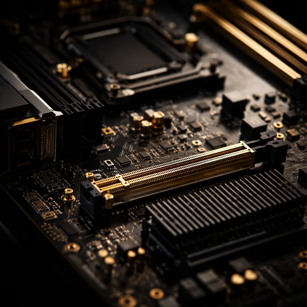
PCIe is the backbone of every compute platform, servers, AI accelerators, SSDs, network cards, and industrial PCs. But unlike older parallel buses, PCIe Gen4 and Gen5 links are analog problems: at 16 and 32 GT/s, the copper trace itself becomes the bottleneck. A link that passes on paper can train down a generation, fail to train at all, or burn weeks of debug time because of a routing decision made in layout.
This guide covers the full PCIe PCB design chain. Channel loss budgets per generation, the 85 Ω differential rules, laminate selection, length matching, via and backdrill strategy, retimer placement, and the DFM checklist your fabrication partner needs to hit your impedance and loss targets. Huaxing PCBA builds high-layer-count boards up to 32 layers with impedance control at ±5%, so the numbers below are the ones we actually verify on the coupon. If you are new to high-speed stackup design, start with our stackup design guide before specifying the layer structure.
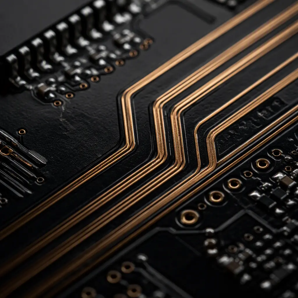
The PCIe Generations: Data Rates, Modulation, and Loss Budgets
Every PCIe generation doubles the data rate, which doubles the signal frequency and shrinks the time budget for reflections and loss. The channel loss budget, the total insertion loss the link can tolerate from connector to receiver, is the single most useful number for PCB design, because it tells you how much of the budget your routing can consume.
| Generation | Data Rate | Signaling | Channel Loss Budget | Nyquist Frequency |
|---|---|---|---|---|
| PCIe 1.0 | 2.5 GT/s | NRZ | ~16 dB | 1.25 GHz |
| PCIe 2.0 | 5 GT/s | NRZ | ~16 dB | 2.5 GHz |
| PCIe 3.0 | 8 GT/s | NRZ | ~16 dB | 4 GHz |
| PCIe 4.0 | 16 GT/s | NRZ | ~23 dB | 8 GHz |
| PCIe 5.0 | 32 GT/s | NRZ | ~34-35 dB | 16 GHz |
| PCIe 6.0 | 64 GT/s | PAM4 | ~42 dB | 32 GHz |
Two things matter here. First, the budget is measured at the Nyquist frequency, the fundamental of the signal, so Gen5 at 16 GHz is four octaves harder than Gen3 at 4 GHz. Second, the budget includes the connector, the package, and the receiver: typically 60-70% of the budget is gone before your board trace even starts. A practical rule used by most design teams: keep the total board trace loss under roughly 10 dB for Gen4 and under 8 dB for Gen5, then verify with simulation. The physics behind this, dielectric loss, skin effect, and impedance discontinuities, is covered in our signal integrity guide.
Key Takeaway: Design against the loss budget, not against a trace length. Two identical-looking 8-inch routes can differ by 3-4 dB depending on laminate, copper roughness, and via count. Which is the difference between a Gen5 link and a Gen4 fallback.
The 85 Ω Differential Pair: Rules That Apply to Every Lane
PCIe specifies 85 Ω ±10% differential impedance . Not the 100 Ω used by Ethernet and USB. This is a common mistake when designers reuse library rules from other protocols.
Design the geometry, then let the fab tune it
Differential impedance is set by trace width, spacing, dielectric thickness, and copper weight. Start with your stackup's reference values (typically 4-5 mil width, 6-8 mil spacing on a 100 µm prepreg layer), then let the factory's impedance calculator converge the final width. What matters at the end is the measured coupon value, not the drawn width. Our impedance control guide explains how tolerance is achieved and verified.
One continuous reference plane, no splits
Every PCIe lane needs an uninterrupted ground reference directly beneath it. A plane split under a differential pair causes an impedance discontinuity and common-mode noise that no termination can fix. If a split is unavoidable, route the pair across it perpendicular to the split with stitching vias on both sides, but treat this as a design failure, not a solution.
Keep the pair coupled
Once a differential pair is routed together with consistent spacing, keep it that way. Fanning the pair apart for component escape changes the odd-mode impedance and creates skew. The exception is intentionally decoupling near connectors for AC coupling caps, where the geometry change is short and symmetric on both signals.
Stackup and Laminate Selection: Matching Material Cost to Generation
Laminate choice is the highest-leverage decision for high-speed PCIe. The loss tangent (Df) of the dielectric, plus the roughness of the copper foil, dominate trace loss above 4 GHz. The table below maps material classes to PCIe generations. And to cost, because upgrading every layer of a 16-20 layer board is expensive.
| Material Class | Typical Df (at 10 GHz) | Reliable Through | Relative Cost |
|---|---|---|---|
| Standard FR-4 | 0.018-0.022 | PCIe Gen1-Gen3 | 1.0x |
| Mid-loss (e.g. FR-4 variants) | 0.008-0.012 | PCIe Gen4 | 1.2-1.5x |
| Low-loss (e.g. Megtron-6 class) | 0.002-0.004 | PCIe Gen5 / Gen6 | 2-3x |
| Ultra-low-loss (PTFE/ceramic) | <0.002 | 56+ Gbps SerDes | 3-5x |
A hybrid stackup, low-loss material on the outer routing layers where the PCIe lanes run, standard FR-4 for power and inner layers, captures most of the signal benefit at a fraction of the cost. Specify this explicitly in your stackup drawing; a factory quote will otherwise default to all-FR-4 or all-high-end material. The full selection criteria, including glass weave and Dk stability, are in our laminate selection guide.
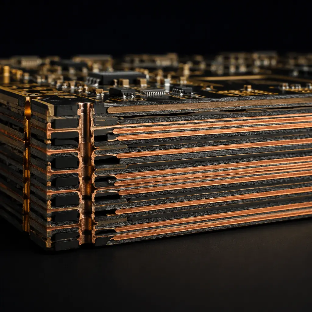
Copper roughness is the second lever. Standard electrodeposited (ED) foil has a rough matte side that adds conductor loss at high frequency. Smooth foil (low-profile or RTF foil) reduces loss by 10-20% on long routes and is worth specifying for Gen5 layers. Ask your fab for the foil profile (Rz value). A 2 µm drop in Rz can save 1-2 dB on a 10-inch trace.
Routing Rules: Length Matching, Skew, and Reference Planes
PCIe is more forgiving than some protocols on absolute length. What matters is skew between the two signals of a pair, and between lanes of a link.
Intra-pair skew: 5 mil (Gen3), 2-3 mil (Gen4/5)
Skew between P and N converts differential signal into common mode, directly eating the receiver's timing budget. Match the two traces of every pair to within 5 mil for Gen3 and tighten to 2-3 mil for Gen4 and Gen5. Add length compensation in the form of small, symmetric serpentines, never add a jog to one trace only.
Lane-to-lane skew: 15-20 mil, and mind the refclk
Skew between lanes matters less electrically but complicates receiver training if it is large. Keep all lanes of a link within 15-20 mil. The 100 MHz reference clock is a differential pair too, route it with the same discipline and keep it away from high-swing switching signals.
Minimize vias per segment
Each via adds a stub and a discontinuity worth roughly 0.5-1 dB at 16 GHz. Limit PCIe traces to two via transitions (e.g. top to inner, inner to bottom) and backdrill or use via-in-pad for any via on a Gen4+ signal path. Via design options are compared in our via technology guide.
Via Optimization and Backdrilling for Gen4 and Beyond
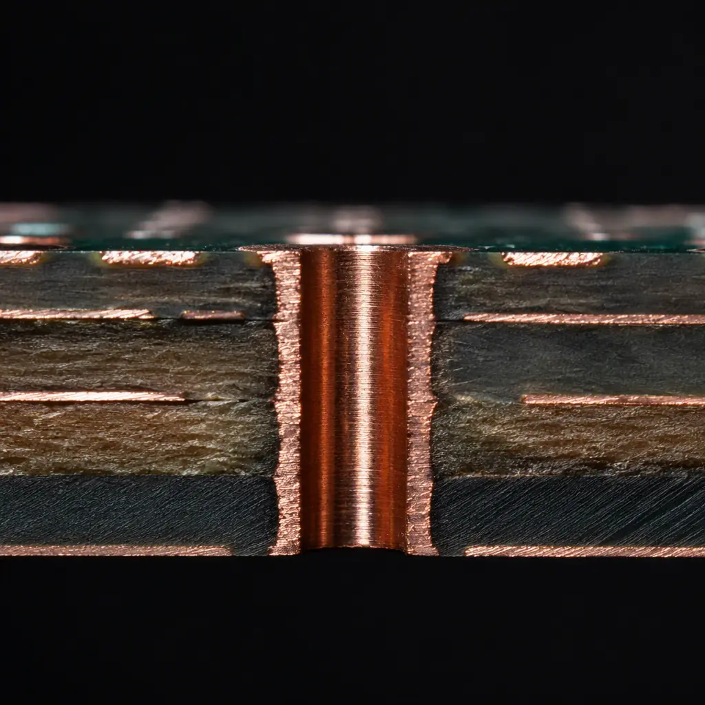
Through-hole vias on high-speed lanes are the classic silent killer. The unused barrel below the signal layer, the stub, resonates and reflects energy back into the channel. At 8 GHz (Gen4) a 30 mil stub already costs measurable loss; at 16 GHz (Gen5) it can push a marginal link over budget.
Backdrill anything on a Gen4+ signal path
Backdrilling removes the unused barrel, leaving a residual stub of typically 5-10 mil depending on drill registration. Specify the target residual stub length and the layer transition points in your fab notes; the fab controls depth with a secondary drill pass. Our backdrilling guide covers the process, tolerances, and cost impact.
Via-in-pad with filled vias for BGA escape
For PCIe switch or root-complex BGA breakouts, via-in-pad with conductive fill removes the stub entirely and keeps plating inside the pad. This is a premium process. Verify your fab supports it on the layer count you are using. Alternative: microvia transitions (HDI) from the pad to inner layers, which naturally keep stub length near zero.
Connectors, Breakout, and Component Placement
Connector selection and placement are part of the electrical channel. A cheap edge-card connector with long pins can consume 2-3 dB of the budget before the trace starts.
Use the connector's recommended footprint, verbatim
PCIe slot, M.2, OCuLink, and U.2 connectors all publish escape patterns with anti-pad and reference-plane cutouts. Deviating from them shifts the connector impedance away from 85 Ω. Keep the trace-to-connector transition short and symmetric. Our high-speed connector guide covers footprint and breakout rules for the common families.
AC coupling caps: 0.1 µF, close to the transmitter
PCIe requires AC coupling on every lane (typically 75-200 nF, with 0.1 µF the common value). Place the caps within roughly 500 mil of the transmitter side, orient identically on both signals, and route the short differential stubs symmetrically. Staggered placement of caps across lanes is fine; asymmetric cap pads within a pair are not.
Redriver or retimer: decide by budget, not habit
A redriver applies fixed equalization, cheap, no protocol awareness, good for recovering 3-6 dB of loss. A retimer re-times the signal and can recover 10+ dB, which is why Gen5 channels longer than ~30-40 inches of total path almost always need one. Place the device at the point of maximum loss, typically mid-channel, and budget its own power and clocking (often a 100 MHz refclk input). Server-class boards show both approaches, see our data center server PCB guide for a real-world architecture.
PCIe 6.0: How PAM4 Changes the Rules
PCIe 6.0 moves from NRZ to PAM4, sending two bits per symbol at 32 GBaud to reach 64 GT/s. PAM4 has three eye openings instead of one, each roughly one-third the height of an NRZ eye. Which is why the loss budget grows to ~42 dB and the material and via requirements tighten further. Design implications: low-loss laminates on every signal layer, backdrill or via-in-pad on all PCIe vias, and receiver DSP equalization becomes mandatory. PAM4 also makes the channel more sensitive to crosstalk, so 3W spacing between aggressive pairs and shield vias at parallel-run boundaries are strongly recommended.
What Your PCB Factory Needs From You: The DFM Checklist
High-speed designs fail at manufacturing handoff in predictable ways. The board is only as good as the agreement between your stackup drawing and the fab's capability. Send these five items with your Gerbers:
Explicit stackup with impedance targets per layer pair
State 85 Ω ±10% differential and 50 Ω single-ended targets, plus the material grades per layer. Ambiguity here produces coupons that miss by 5-8 Ω and links that train down.
Impedance coupon placement
Request coupons on each high-speed layer pair, placed near the board edge on the production panel, and specify that measured values be included in the report. Do not rely on a single coupon from one layer.
Backdrill depth and residual stub requirements
Define which nets are backdrilled, the target residual stub (e.g. ≤ 10 mil), and which layer transitions apply. Confirm the fab's depth-control tolerance before approving the quote.
Via-in-pad / HDI confirmation
If you use via-in-pad or microvia escape, confirm the process on the specific layer count and board thickness, some combinations require sequential lamination. HDI capability details are in our HDI technology guide.
Test requirements beyond flying probe
For Gen4+ boards, ask about TDR verification of impedance and, where feasible, loss measurement on a test coupon. Standard electrical test verifies connectivity, not signal quality, the distinction is covered in our testing methods guide.
Key Takeaway: PCIe Gen4/Gen5 success is decided at the intersection of design and fabrication: laminate class, foil roughness, via strategy, and impedance verification. Write the stackup and DFM requirements down before quoting, and make the fab's measured coupons part of the acceptance criteria.
Summary: The PCIe Design Checklist
Budget first
Compute the channel loss budget for your generation; keep board trace loss under ~10 dB (Gen4) or ~8 dB (Gen5).
85 Ω everywhere
Differential pairs at 85 Ω ±10%, continuous ground reference, matched to 2-5 mil within the pair.
Material matched to speed
Mid-loss for Gen4, low-loss for Gen5/6, smooth foil on high-speed layers, hybrid stackup to control cost.
Vias: backdrill or fill
Backdrill all Gen4+ signal vias to ≤10 mil residual stub; via-in-pad for BGA escape.
Verify at the fab
Impedance coupons per layer pair, TDR where available, DFM review before production.
At Huaxing PCBA, we build high-speed boards up to 32 layers with ±5% impedance control, low-loss laminates, backdrilling, and via-in-pad processes, and we report measured coupon values with every batch. Send us your stackup and Gerbers for a free DFM review that checks impedance targets, via strategy, and manufacturability before you commit to production. Contact our engineering team or read our signal integrity guide to go deeper on the electrical side.
