
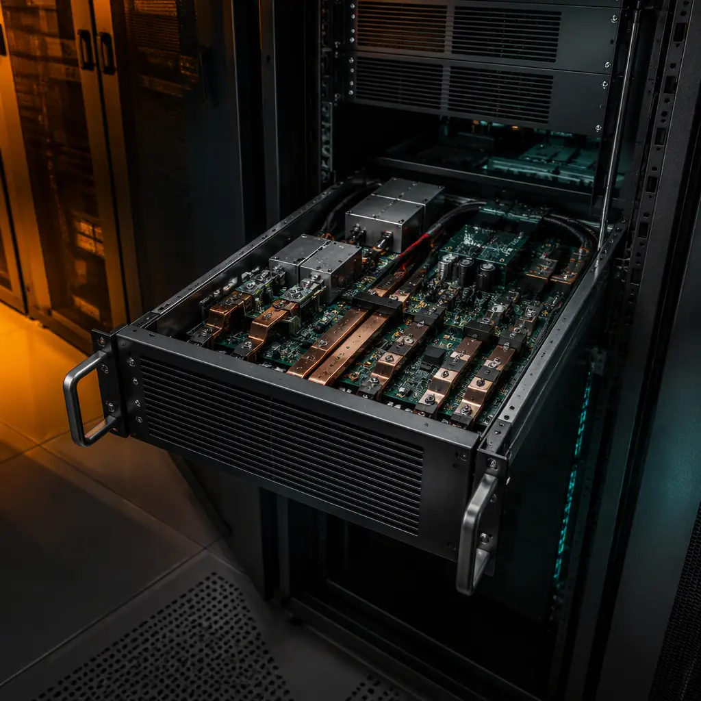
A UPS sits between the mains and the equipment that must never lose power: hospital monitors, factory PLCs, server racks, cash registers and security systems. Every one of those boxes, from a 500 VA desktop unit to a 200 kVA three-phase cabinet, is built around the same three power functions, rectifier, inverter and battery charger, and they all live on PCBs that carry tens to hundreds of amps.
The board is where UPS reliability is won or lost. A power module that runs at 40°C ambient for 10 years will see more than 87,000 hours of thermal cycling, continuous vibration from fans, and switching currents that stress every solder joint and trace. Huaxing PCBA fabricates and assembles UPS power boards with up to 6 oz copper on the current-carrying layers, and this guide walks through the layout and manufacturing decisions that separate a 10-year product from a warranty claim.
UPS Topologies and What Each Means for the PCB
The topology determines how much current the board must carry and how hard the power stage works. There are three mainstream designs, and each places different demands on copper weight, thermal management and isolation:
| Topology | Transfer Time | Typical Efficiency | PCB Demand |
|---|---|---|---|
| Standby (offline) | 4–10 ms | 97–98% | Low, inverter rarely runs |
| Line-interactive | 2–6 ms | 95–97% | Medium, boost converter + inverter |
| Double-conversion (online) | 0 ms | 92–96% | High, full power always flows through rectifier + inverter |
Double-conversion units are the bulk of the commercial and industrial market because they isolate the load from every mains disturbance. The incoming AC is rectified to a DC bus, then inverted back to clean AC. That means the rectifier and inverter stages each handle 100% of rated power continuously, so the PCB is effectively two power boards sharing one substrate. Our power electronics PCB guide covers the general high-power layout rules; below are the UPS-specific decisions.
Key Takeaway: Topology choice is a PCB decision, not just a marketing one. If you spec a double-conversion UPS, the board must be designed for continuous full-load heat. Copper weight, via arrays and base material grade are non-negotiable.
Power Stage Layout: Rectifier, Inverter and the High-Current Paths
In a 10 kVA single-phase UPS with a 400 V DC bus, the inverter output stage carries roughly 25 A RMS. The battery path is worse: a 48 V battery bank feeding the same unit draws 200 A+ at full load. Those numbers define the layout.
Heavy copper for the DC bus and battery traces
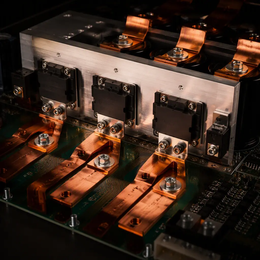
The battery and inverter high-current paths need 3–6 oz copper on outer layers and 2–3 oz on inner layers, or busbars for anything over ~100 A. At 200 A, a 3 oz trace needs to be roughly 25–40 mm wide depending on allowable temperature rise: usually impossible on a dense board, which is why busbars or copper straps bridge the battery connector to the inverter. See our heavy copper PCB guide for plating and etching limits, and trace width vs current capacity for the calculation method.
IGBT/SiC switching cell kept tight and symmetric
The inverter half-bridge (or full-bridge) switching cell must be a compact loop: gate drivers within 5–10 mm of the device, snubber capacitors across the DC bus right at the module pins, and Kelvin-connected emitter/current-sense traces. Stray inductance in this loop causes voltage overshoot that destroys the switches; 16–20 kHz IGBT switching is standard, with SiC MOSFETs pushing toward 100 kHz in newer designs. Our SMPS layout guide details the switching-loop rules that apply identically here.
Isolation and creepage for the mains side
Anything connected to 230 VAC mains needs reinforced isolation from the low-voltage control side: minimum 8 mm creepage between mains and SELV circuits (IEC 62368-1), 2.5 mm for basic isolation at 230 V, and a slot or routed gap where creepage alone cannot be achieved. The control and gate-drive sections belong on the opposite side of the board from the mains entry, with optocouplers or digital isolators crossing the boundary.
Thermal Management: Where UPS Boards Die
A double-conversion UPS dissipates 3–5% of its rated power as heat in the power stage. A 10 kVA unit therefore needs to move 300–500 W out of the enclosure continuously. The PCB is the first link in that chain, and it fails in predictable ways.
Thermal via arrays under every power device
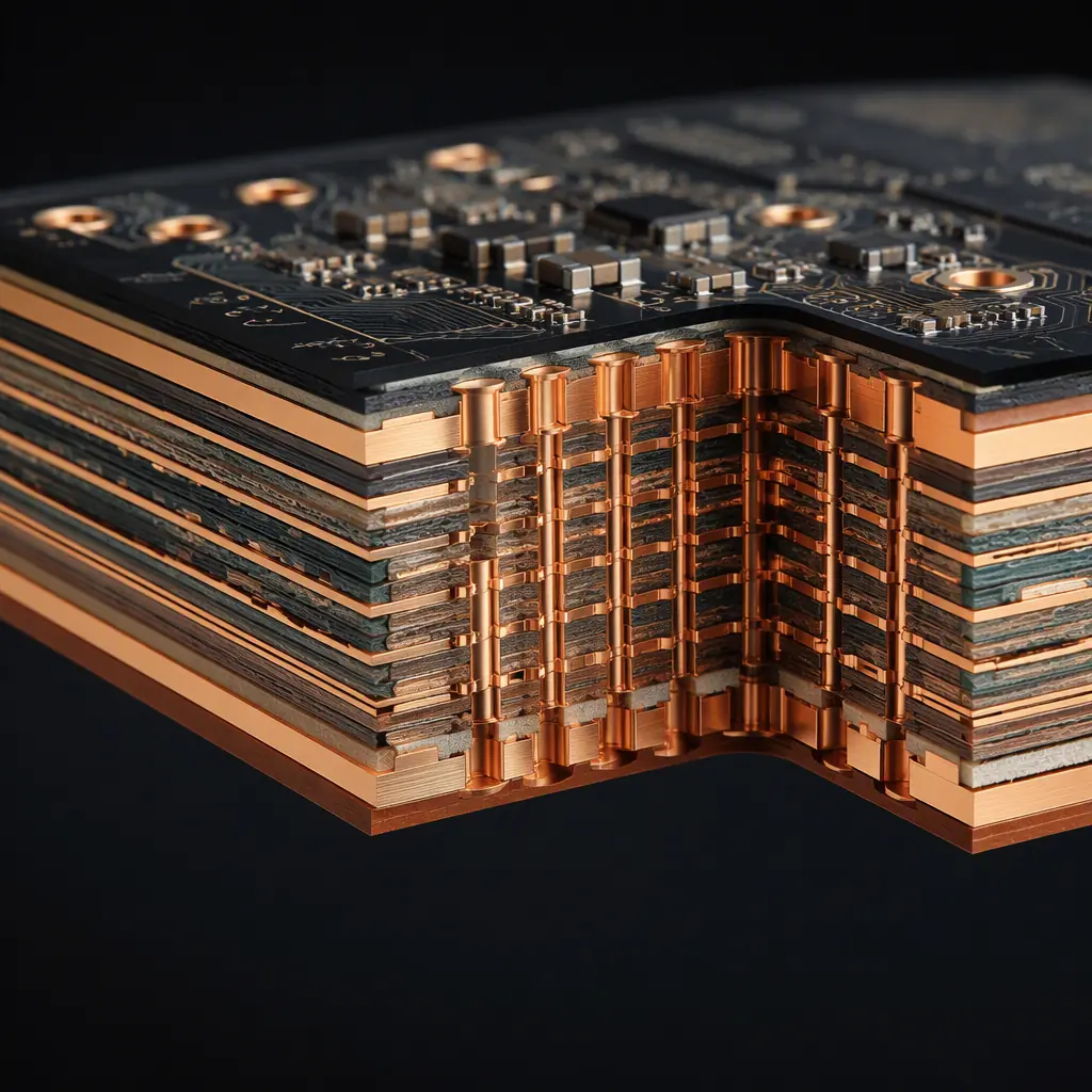
Each IGBT or MOSFET pad needs a dense array of 0.3 mm vias on 0.6–1.27 mm pitch to conduct heat into inner copper planes. Filled or tented vias under the pad keep solder from wicking away during reflow. A 25×25 mm device footprint should carry 50–150 thermal vias. This is the cheapest thermal solution in the BOM and the most commonly under-specified one. Our thermal management guide covers via sizing and plane strategies in detail.
High-Tg base material, non-negotiable
Continuous operation near 100°C board temperature requires at least 170°C Tg laminate (mid-Tg FR-4 at 150°C is marginal), and 180°C Tg for the hot zones. The base material choice also drives CTE match with the heavy copper. Differential expansion between thick copper and laminate is a primary cause of delamination in power boards. Laminate selection logic is covered in our PCB materials guide.
Heatsink interface and airflow direction
Devices that bolt to heatsinks should sit near the board edge or in a defined airflow lane, with the heatsink mounting holes carrying clean copper to the planes (no tented vias under the screw pad). Fan-cooled UPS designs need the board's tall components, electrolytic capacitors, transformers, oriented so they do not block the flow path. Battery-side capacitors are the first components to dry out in a hot enclosure; derate their lifetime at the expected operating temperature.
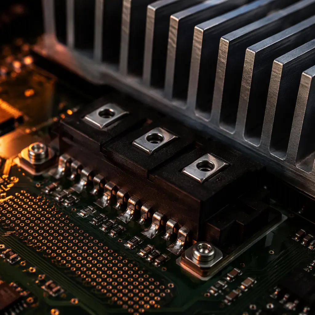
Reliability Reality: The most common field failure in UPS boards is not the silicon. It is the thermal path around it: under-sized via arrays, marginal laminate, or capacitor banks cooked by proximity to the heatsink. Design the board for the enclosure's worst-case ambient, not the lab bench.
Battery Charger, Monitoring and the Static Bypass
Beyond the power stage, three subsystems dominate the rest of the board area and most of the control firmware.
Charger: constant current then constant voltage
Sealed lead-acid banks charge at C/10 or C/20 constant current, then float at 2.27 V/cell (13.6 V per 12 V block). Li-ion UPS packs use CC/CV with a much tighter voltage window and need cell-balancing and protection on the board itself. The charger section is a second power stage, it gets the same copper-weight and thermal treatment as the inverter, scaled to its lower current. Our energy storage PCB guide covers battery-management layout for both chemistries.
Static bypass: the SCR/thyristor path
When the inverter faults, the static bypass switch transfers the load directly to mains in milliseconds. The bypass path must be physically separate from the inverter output on the board, its own traces, its own connectors, so a failed inverter cannot back-feed the bypass. High-current bypass designs again lean on busbars; 10 kVA-class units switch 40 A+ through the bypass.
Sense and control: keep them out of the power loops
Voltage and current sense traces are the eyes of the control loop. Route them as differential pairs away from switching nodes, or the 20 kHz switching noise becomes measurement error and the inverter's output regulation suffers. The MCU and gate-drive supply should be fed from a quiet rail, not tapped off the noisy DC bus without filtering. Board-level EMC practice for this kind of mixed power/control design is in our EMI/EMC design guide.
Manufacturing UPS Boards: Copper, Testing and Certification
UPS boards combine heavy copper, mixed SMT/through-hole power components and safety-critical isolation, a combination that needs specific manufacturing controls.
Heavy-copper fabrication limits
Above 3 oz, minimum trace width and spacing grow, and etching becomes less precise, plan 0.3 mm minimum trace/space at 3 oz and wider at 4–6 oz. Mixed-weight boards (heavy copper on power layers, 1 oz on signal layers) are standard for UPS: the stackup must be planned so the heavy layers do not distort the board during lamination. Our heavy copper guide lists the practical design rules.
Hi-pot, burn-in and thermal cycling tests
Every production unit gets a hipot test: typically 1500 VAC or 2121 VDC for one minute between mains and SELV (IEC 62368-1), plus functional load testing. Power boards benefit from burn-in at elevated temperature and from thermal cycling to expose marginal solder joints on the heavy components. Test coverage strategy is compared in our PCB testing methods guide, and burn-in/ESS practice in the burn-in and ESS guide.
Certifications to design for from day one
UPS products are certified to IEC 62040 (UPS performance), IEC 62368-1 (safety), and in North America UL 1778. Certifications are board-level decisions: creepage, component spacing, thermal stress ratings and flammability class are locked in at layout time. Our UL certification guide and certifications overview map the requirements to design actions.
Summary: The UPS Board Checklist
Specify the topology honestly, then design the board around its worst case: heavy copper and busbars for the battery path, a tight switching cell with snubbers, thermal via arrays under every power device, 170°C+ Tg laminate, 8 mm mains creepage, and a physically separate static bypass. Validate with hipot, burn-in and thermal cycling before the first production run.
At Huaxing PCBA, we fabricate UPS power boards with 6 oz copper, 180°C Tg laminate and 32-layer stackups, and assemble them across 8 SMT lines with selective soldering for the through-hole power components. Our engineering team reviews current capacity, thermal via arrays and isolation gaps during the free DFM check. Read our EV charger and DC-DC converter guide for related power-conversion layout rules, or contact us with your UPS design for a manufacturing review.
