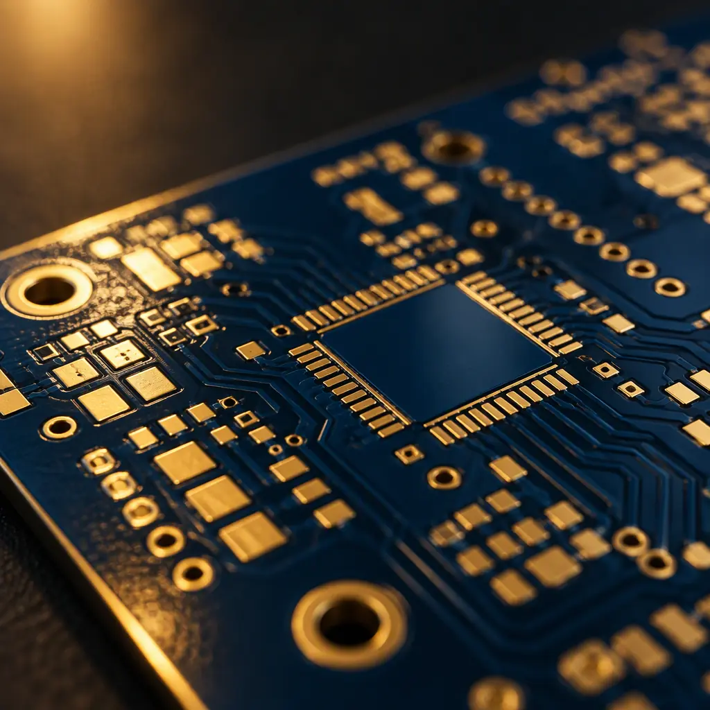
Every assembly drawing specifies solder mask. Almost none of them specify all three of the properties that decide whether the mask passes or becomes a defect source: the mask system itself, the thickness the fabricator will actually apply in each region, and the registration tolerance between the mask openings and the copper they expose. The result is the most common gap in PCB purchase specifications — a double-sided board with SMD pads, test points and press-fit holes can need three different mask callouts, and a single "green LPI" note cannot express them. This guide covers what LPI, dry film and UV-curable ink actually deliver, the thickness numbers that matter for impedance and solder dams, and how registration tolerance translates into vendor selection.
The Three Mask Systems and Where Each Belongs
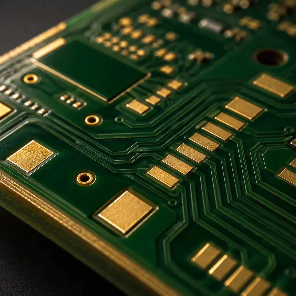
The industry has settled on three families, and the choice is driven by copper height, resolution and volume rather than by preference:
| System | Applied thickness over trace | Best for | Hard limits |
|---|---|---|---|
| LPI (liquid photoimageable), screen or curtain coated | 15–25 µm on 1 oz trace; 25–40 µm on 2 oz | The default for 95% of boards; fine pitch, dense routing, multilayer | Thin over heavy copper; needs good planarisation to hold thickness |
| Dry film photoimageable | 25–50 µm, uniform by lamination | Heavy copper, thick traces, high-current boards | Coarser resolution; difficult on dense fine-pitch features; higher cost |
| UV-curable ink (screen printed, no imaging) | 20–35 µm, pad openings by screen | Low-density single-sided boards, cheap consumer products, quick-turn prototypes | Pad opening resolution limited by screen; poor registration on small pads; not suitable below 0.5 mm pitch |
The failure mode that follows from this table is specifying LPI on a 4 oz heavy-copper power board. The coating has to cover a very tall trace, and normal spray or curtain application produces a mask that is thin over the trace crowns — sometimes under 10 µm — and prone to cracking during thermal cycling. Dry film, laminated at a controlled thickness, is the correct answer there, and it should be on the drawing before the quote rather than discovered at first-article.
Thickness: Two Numbers, Not One
When a specification says "solder mask thickness 25 µm", it is almost always quoting the thickness over a bare laminate area or over a thin trace. That number is real but rarely controlling. What controls performance is thickness in two specific places:
- Over the trace crown, on impedance-controlled boards. The mask sits in the field of the microstrip or coplanar waveguide and changes the effective dielectric constant. A 20 µm mask over a 100 µm trace shifts impedance by only a fraction of an ohm; a 40 µm mask plus a big overlay can move it several ohms. For ±5% impedance control, the mask thickness should be specified as a range and included in the field solver model, not treated as an afterthought.
- Between adjacent pads, as a solder dam. The dam height and width decide whether the mask contains molten solder during reflow. A dam that is too thin gets wetted by solder and no longer separates the pads; a dam that is too narrow is removed by the etchant or by poor development. The practical requirement is a dam width of at least 0.1 mm between pads at 0.5 mm pitch, taller than the finished copper it separates.
The related numbers for coat weight on the finished surface — which matter far more than the on-trace figure for cosmetic and insulation reasons — are covered in solder mask thickness and registration.
Registration Tolerance and Vendor Selection

Mask registration is the offset between the mask opening and the pad it exposes. It is the single property that most reflects a fabricator's process control, and it is invisible in a quotation. The industry-standard figure is roughly ± 75 µm for standard LPI processing, with tighter capability — around ± 50 µm — on the fine-pitch lines used for HDI.
What happens when registration drifts is worth understanding because it changes the failure mode, not just the quantity of defects:
- Positive offset (mask opening larger than pad). Copper is exposed beyond the pad edge on one side. On a fine-pitch part this reduces the solder dam, and on a BGA it exposes trace that should have been covered — a short risk at reflow.
- Negative offset (opening smaller than pad). The mask overhangs the pad. This is often preferred deliberately — it is the basis of SMD (solder-mask-defined) pads, where the mask aperture sets the joint area — but when it happens uncontrolled it reduces the wettable area asymmetrically, causing tombstoning on small passives and weak heels on fine-pitch leads.
This is why the NSMD vs SMD decision should be an explicit callout on the drawing rather than a fabricator's default. On 0402 and smaller passives, mask-defined pads reduce the risk of solder bridging but make the joint sensitive to registration; non-mask-defined pads give more wettable area but rely on the copper etch tolerance instead. The full trade-off is set out in SMD vs NSMD pads.
Factory reality: on fine-pitch assemblies, mask registration is one of the first things we measure on a new fabricator's sample board, because it predicts first-pass yield more reliably than any other single fabrication attribute. A supplier that cannot hold ± 75 µm on a 0.5 mm pitch board will produce bridging on some lots and starved joints on others, and the fault will appear as an assembly problem rather than a fabrication one.
Colour, Finish and Process Compatibility
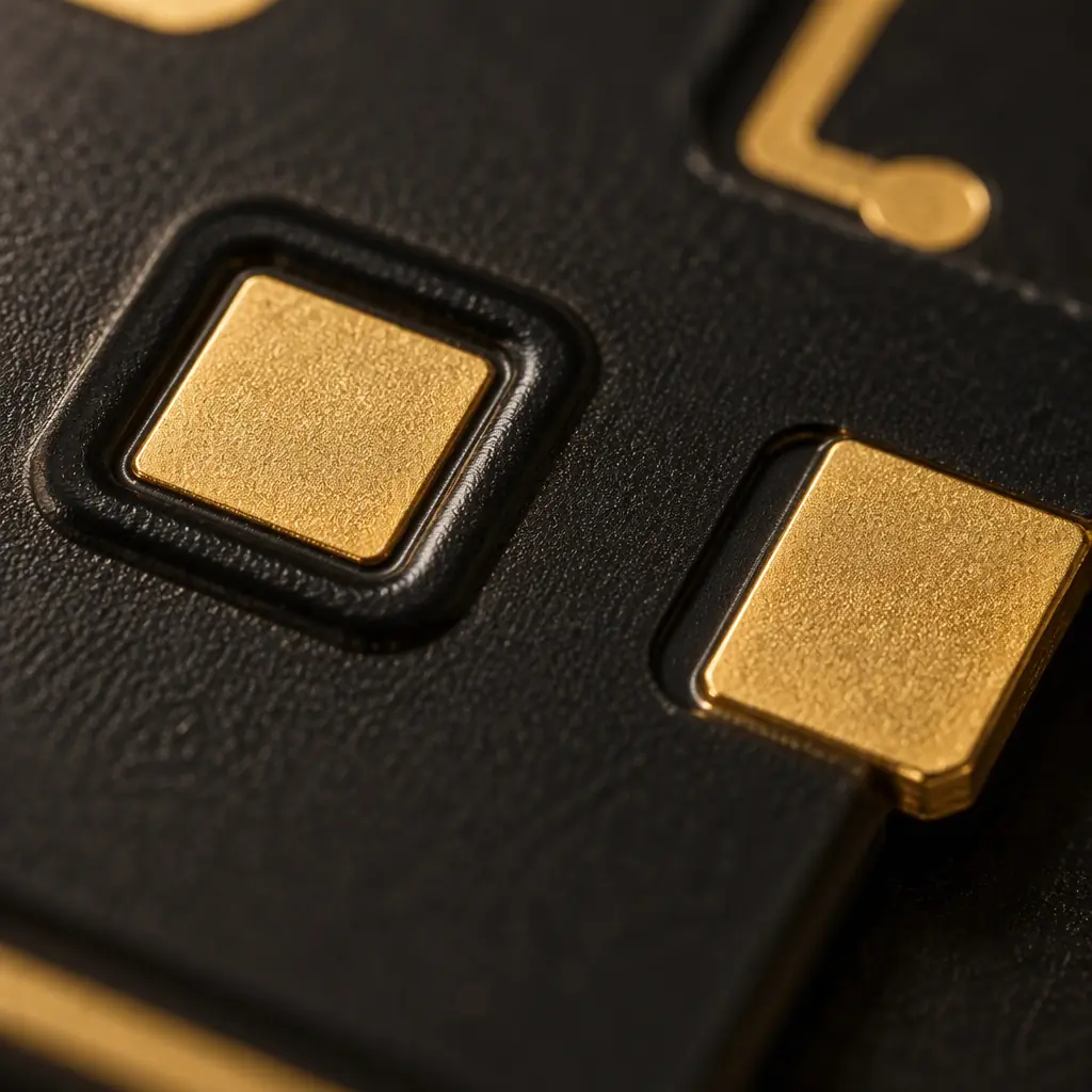
Mask colour is mostly cosmetic but not entirely. The relevant differences for a buyer:
- Green remains the most forgiving and the cheapest, because the process windows are the widest and inspection contrast is well established. Where there is no aesthetic requirement, it is still the default worth choosing.
- Black and matte black have narrower development windows and show residue and scratches more than green. They are common on consumer product boards where appearance matters.
- White is standard for LED boards, where reflectivity matters, and is often specified with a matte finish for outdoor luminaires.
- Blue, red, purple are all routine, with the same process considerations as black.
Two compatibility rules matter more than colour. First, mask must cure compatibly with the surface finish: an ENIG finish applied after mask cure needs a mask that survives the nickel and gold baths, and a silver or OSP finish needs a mask whose cure does not contaminate the pad. Second, mask type affects high-frequency performance — the dielectric constant and loss of the mask film become part of the transmission line. On designs above about 10 GHz, the mask over controlled-impedance traces is a modelled layer, and the fabricator must supply its dielectric properties. The broader material context is in PCB solder mask types and the finish interaction in surface finish selection.
What to Write on the Drawing
A complete mask callout is five lines, and all five are cheap to add at design stage:
- System: LPI, dry film, or UV ink, by name.
- Colour and finish (gloss or matte), including any requirement that the colour matches a previous build.
- Thickness requirement over trace crown and in the solder dam regions, as ranges rather than single values.
- Pad definition: NSMD by default, with specific parts called out as SMD, and the pad dimensions adjusted accordingly.
- Registration tolerance in micrometres, and the finest pitch on the board, so the fabricator can judge whether the job belongs on its standard or fine-pitch line.
Specifying items two through five on the first quotation avoids the most expensive kind of mask problem: one that only appears after a production run, when the boards are already assembled and the root cause sits in a fabrication process nobody specified. The related design considerations for mask openings around vias and test points are in DFM tips, and where the mask interacts with the assembly process through stencil apertures, see SMT stencil aperture design.
At Huaxing PCBA, LPI solder mask is applied and imaged in-house on 32-layer capable lines, with dry film available for heavy-copper builds and registration held to ± 75 µm standard and ± 50 µm on fine-pitch work. We build to IPC-6012 Class 2 and 3 and assemble across 8 SMT lines. Send your stackup and mask requirement for a quote or ask an engineer whether your mask callout will hold on the pitch you have specified.