
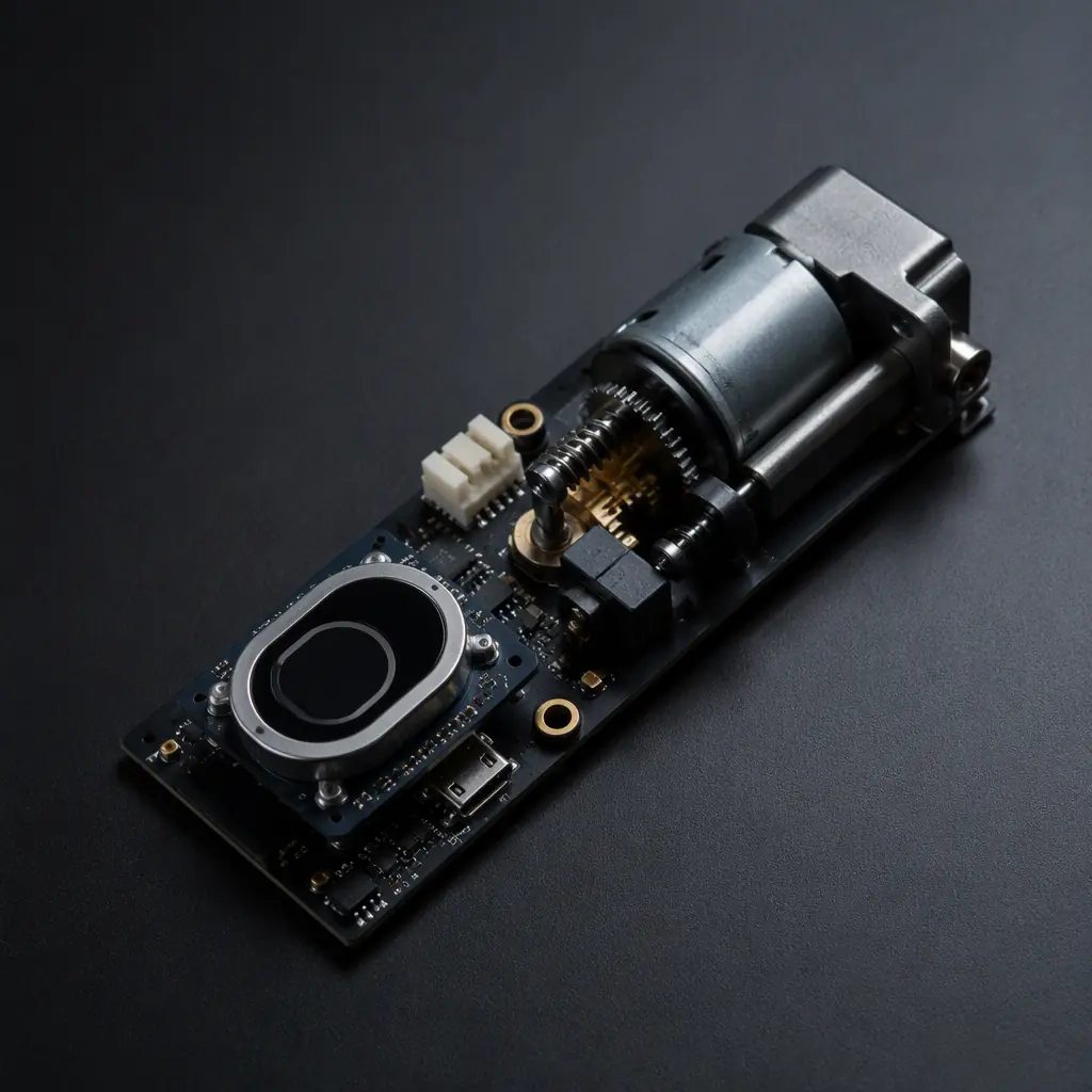
A smart lock is a battery-powered product with a 6–12 month battery life target, a motor that must move a deadbolt against real-world friction, and a security requirement that never sleeps. Its PCB has to run the whole product on four AA batteries or a small Li-ion pack, deliver 2–3 A bursts to a geared DC motor for the 200–500 ms it takes to throw the bolt, read a fingerprint through a flexible cable, and keep a secure element powered and tamper-aware at all times. Every one of those jobs is a layout and component decision.
This guide covers the four sections that decide smart lock quality: the geared DC motor drive and stall handling, capacitive fingerprint sensor integration, ultra-low-power battery design and the sleep/wake architecture, and the secure element with tamper resistance. It closes with the manufacturing and test flow for access-control hardware. Huaxing PCBA assembles smart lock and IoT security boards across 8 SMT lines, the same rules apply to our IoT hardware security boards and BLE wireless boards.
Motor Drive: Moving the Deadbolt Every Time
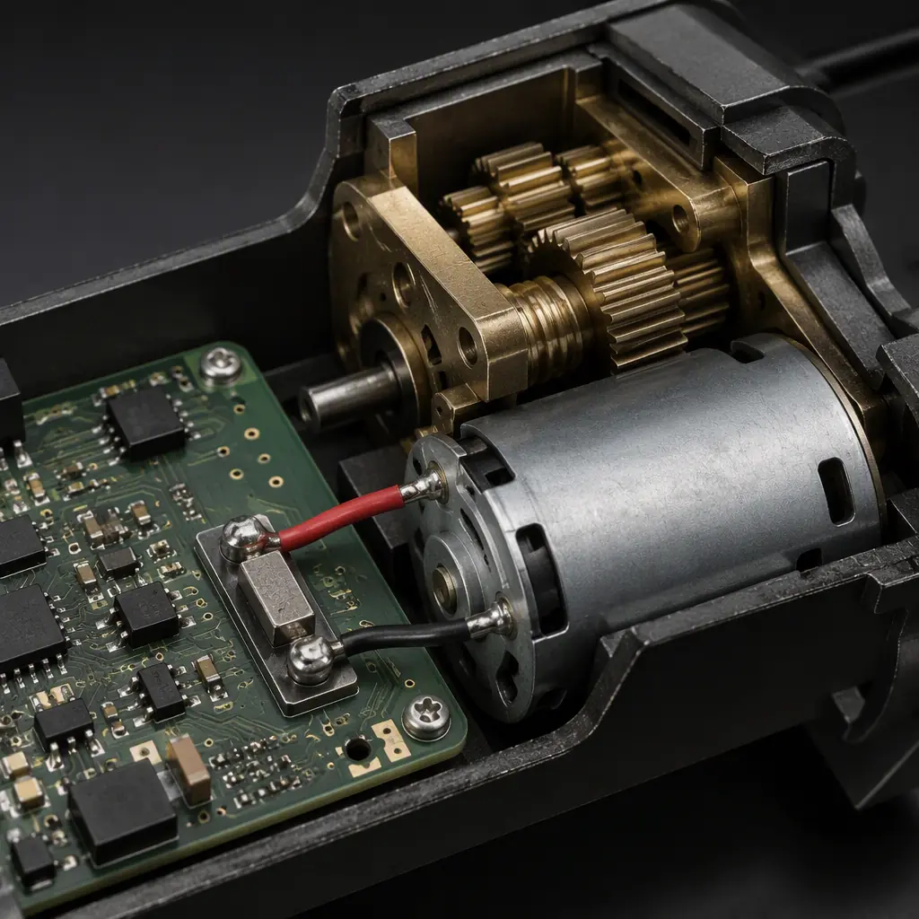
The deadbolt motor is a small geared DC motor (typically 3–6 V, drawing 500 mA–2 A under load). It must throw and retract the bolt reliably for years: including against door frames that swell with humidity and alignments that drift. The drive electronics have to deliver the current, detect when the bolt has fully traveled, and survive a stall without burning out.
H-bridge with current sensing, not just a relay
A relay gives you two positions but no feedback. An H-bridge (two half-bridges, e.g., a dual MOSFET driver) lets the MCU control direction, apply PWM for soft-start, and read motor current through a low-side sense resistor. The sense resistor (10–50 mΩ) feeds a comparator-based stall detector, when current exceeds the stall threshold for more than 50–100 ms, the firmware reverses or stops. This is what prevents a burned-out motor when the bolt hits an obstruction.
End-of-travel detection: current profile beats limit switches
Most smart locks detect full travel by the motor current spike at the mechanical end-stop rather than a limit switch (fewer moving parts, fewer wires to the bolt). The current profile, low during travel, sharp rise at the stop, is read by the MCU's ADC at 1 kHz or faster. The sense resistor and ADC reference must be accurate enough to distinguish a normal end-stop spike from a jam; that is a component tolerance and layout decision, not firmware magic.
Freewheeling and back-EMF protection
When the H-bridge switches off, the motor's inductance generates a voltage spike that can exceed the supply rail. Flyback diodes (or the MOSFETs' body diodes plus a TVS clamp) across each half-bridge are mandatory. The motor traces should be short and paired, with the H-bridge close to the battery input so the 2 A pulse does not sag the digital rail. A brownout during unlock is a common field failure on badly laid-out locks.
Key Takeaway: The motor drive is where smart locks fail in the field. Stall detection, end-of-travel sensing and brownout prevention are hardware decisions. A lock that grinds or dies mid-cycle is almost always a board that skipped them.
Fingerprint Sensing: The FPC Problem
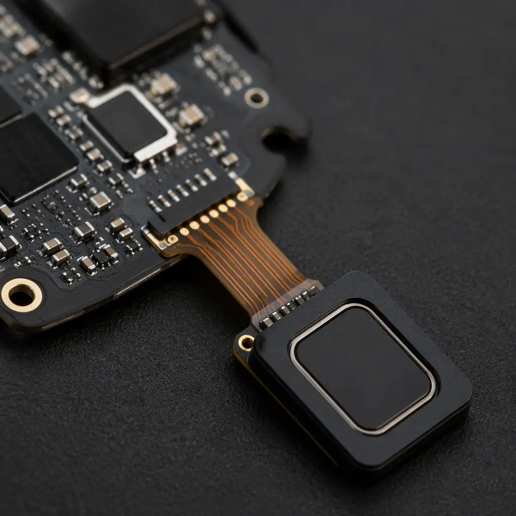
Capacitive fingerprint sensors sit on the exterior of the lock (touchpad side) while the mainboard lives behind the interior escutcheon, connected by a flexible printed circuit (FPC). That cable carries a high-impedance sensor bus through an environment with ESD, moisture and RF from the radio module.
Keep the FPC short and shielded
The fingerprint sensor's analog output is a small capacitance change (femtofarad level). The FPC should be as short as possible, with the sensor's signal lines shielded by a ground plane on the adjacent FPC layer. Route the FPC away from the motor wires. The motor current pulse couples into the sensor bus and can cause false reads or failed matches during the unlock sequence. Our signal integrity guide covers the impedance and shielding rules for sensitive analog buses.
ESD protection at the sensor boundary
The touchpad is the most ESD-exposed point on the product, users touch it after walking on carpet in winter. Every line from the sensor (power, clock, data, reset) needs a TVS array at the FPC connector, with the TVS ground tied directly to the chassis ground point. ESD design for the whole product is covered in our ESD control guide.
Sensor authentication and secure boot path
Modern capacitive sensors include a match-on-chip engine and cryptographic authentication with the host MCU. The sensor's challenge-response lines are security-critical: keep them on dedicated traces, not shared with other peripherals, and route them away from test pads and programming headers that an attacker could probe. The IoT hardware security guide has the full threat model for sensor-to-MCU trust.
Battery Life: Sleep Architecture and Power Budget
A smart lock's power budget is dominated by standby, not by the motor. The motor runs for a few seconds a day; the lock sits in sleep mode for the other 86,000 seconds. The difference between a 6-month and a 12-month battery life is almost entirely the standby current.
Target under 100 µA standby, not "low power"
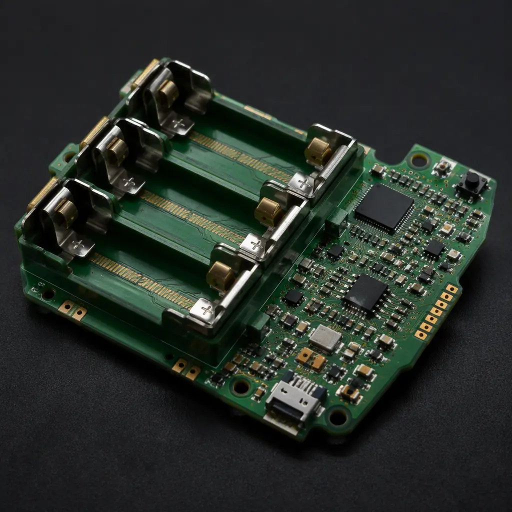
A four-AA (or 4S NiMH / single Li-ion) lock with a 2,500 mAh effective capacity has about 2,000 mAh usable. At 100 µA standby, that is roughly 20,000 hours, about 2.3 years, which covers the 6–12 month spec with margin for motor draws and radio events. Every component in the sleep path must be selected for quiescent current: the MCU in deep sleep (µA range), a wake-on-touch or wake-on-radio circuit that powers the rest, and regulators with enable pins so the fingerprint sensor and radio can be fully unpowered between events.
Design the wake chain: touch → sensor → MCU → radio
The classic architecture has a capacitive touch wake IC or the sensor's own wake output that pulls the MCU from deep sleep; the MCU then powers the fingerprint sensor, authenticates, and only then enables the BLE radio for the unlock command. Each stage powers the next, so idle current compounds only one level deep. The BLE link budget and radio layout that make this reliable are in our BLE PCB design guide.
Measure the real current profile, not the datasheet
Battery life predictions fail on paper. The production test should measure the full current profile, sleep current, wake spike, motor pulse, radio burst, with a logging ammeter, and the firmware team should verify the sleep current on the assembled board, where leakage from a mis-specified pull-up or a leaky TVS shows up. A single 10 µA leak per component across 20 components is the difference between a 12-month and a 6-month lock. The BOM optimization guide covers selecting low-quiescent parts without inflating cost.
Security: Secure Element and Tamper Resistance
Access control hardware is a physical attack target. The secure element stores the keys that authenticate the lock to the user's phone and the home hub, and the PCB layout decides how hard those keys are to extract.
Secure element with mesh and tamper inputs
A dedicated secure element (SE) or secure MCU with a tamper mesh input should hold the keys. The tamper mesh, a fine-pitch grid of traces on the outer board layers that breaks if drilled or scraped, is wired to the SE's tamper pin; any break triggers key erasure. The mesh traces are typically 0.1–0.15 mm on the outer layers with vias that interlock with the inner ground plane, making bypass attempts visible.
Physical separation and shield cans
The SE should sit on the interior side of the board, away from the exterior-facing sensor and the battery contacts, with a grounded shield can over the SE and the MCU's crypto section. The I²C or SPI bus between MCU and SE should be point-to-point (no other devices on the same bus) so an attacker cannot tap a shared bus. Route it on inner layers where practical.
Secure boot and debug-port lockdown
The MCU's debug port (SWD/JTAG) must be disabled or password-protected in production firmware. An open debug port is the fastest key-extraction path. Test pads for the debug port should be removed or covered after programming. The traceability guide covers the programming and serialization flow that ties each lock's keys to its serial number.
Manufacturing and Test for Access-Control Hardware
Smart lock boards need a test flow that covers both function and security. Beyond standard SMT inspection, the lock board typically requires:
| Test | What It Catches | Where It Runs |
|---|---|---|
| ICT / flying probe | Opens, shorts, wrong values | Post-reflow |
| Fingerprint sensor test | Dead sensor, FPC assembly, false reject rate | Functional station, test finger |
| Motor cycle test | Stall detection, end-of-travel, direction | Functional station, loaded bolt fixture |
| Sleep current test | Standby leakage, wake chain | Logging ammeter, per unit |
| RF test (BLE) | Antenna tuning, TX power | Shielded RF chamber |
Test the motor against a loaded fixture
A motor cycle test on a bare bench tells you nothing about real-world friction. The production fixture should load the bolt mechanism (spring-loaded to simulate a door latch) and verify: bolt throws in 200–500 ms, stall detection trips on a blocked bolt, and the lock returns to ready state. Every unit, not samples, this is the core reliability function.
Measure sleep current on every unit
Standby current is the battery life spec, and it drifts with component batches. A per-unit sleep current measurement (with a logging ammeter that captures the full wake profile) catches a bad batch of regulators or a paste-affected TVS before it ships. The PCB testing methods guide covers the functional test station design.
Secure provisioning at the end of the line
Key injection and serialization must happen in a controlled step at the end of assembly, with the debug port locked in the same operation. The provisioning station logs each serial number against its injected keys, and the log is the audit trail for the product's security certification. MSL handling for the sensor and SE during SMT matters too, see our MSL guide for the baking and floor-life rules.
Building a Lock Users Trust for Years
The design order for a smart lock is: motor drive and stall handling first (the reliability core), then the power budget and sleep architecture (the battery life spec), then the fingerprint path and its ESD protection, then the security layout around the SE. Each is a PCB decision that shows up in the field as either a smooth unlock or a support ticket. Verify the motor against a loaded fixture on every unit, measure sleep current per unit, and provision keys in a controlled line step. The locks that earn 4.5-star reviews are the ones whose boards were designed around the motor stall and the 100 µA budget from day one.
Huaxing PCBA assembles smart lock and access-control boards with secure provisioning, loaded-fixture motor testing and per-unit sleep current logging across 8 SMT lines. Read our IoT security guide for the threat model, or send your BOM and battery target . We'll return a DFM review covering the motor drive, power budget and tamper layout with your quote within 24 hours.
