
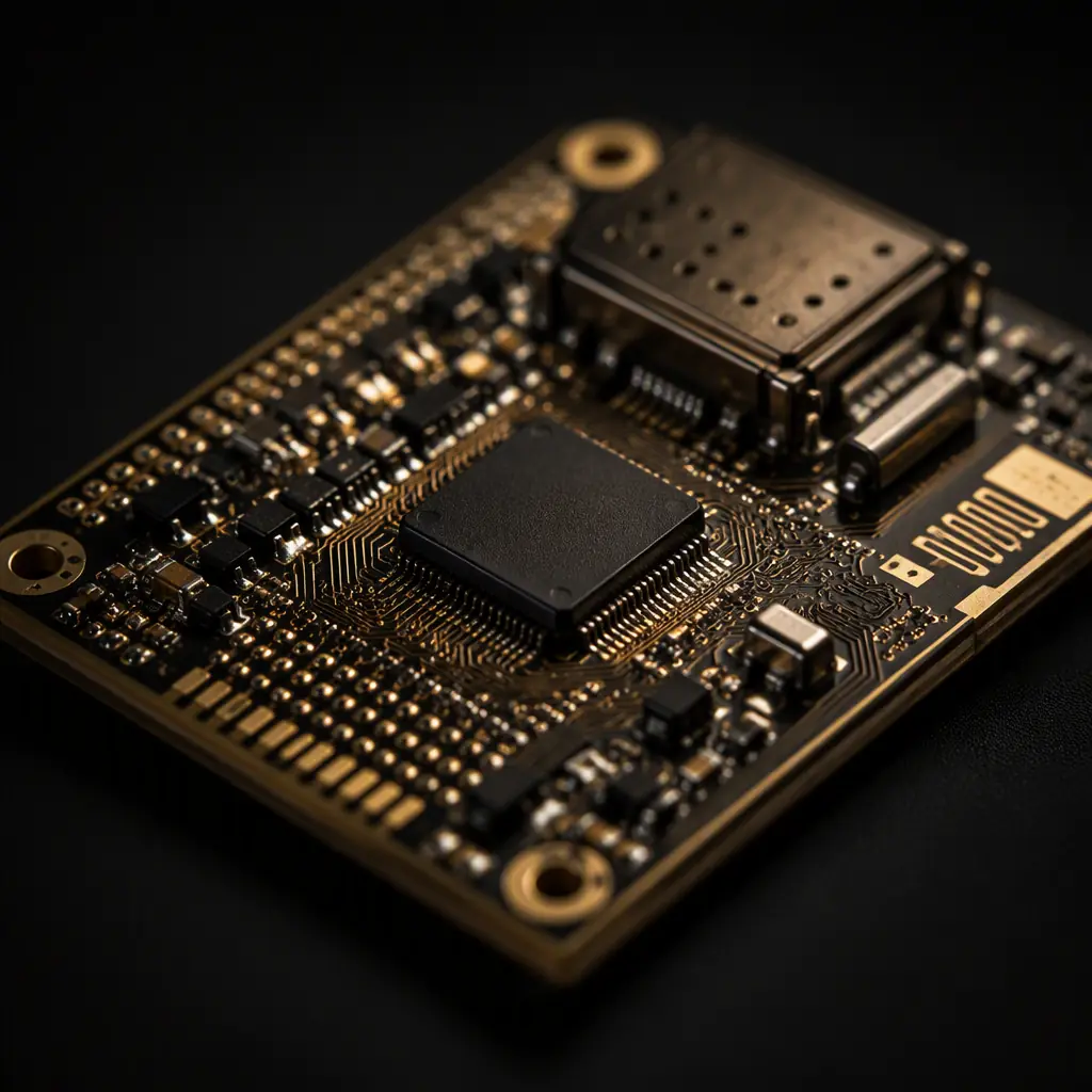
Every connected product eventually holds something worth stealing: payment credentials, device identities, encryption keys, firmware IP, or customer data. Attackers know that software defenses — encryption, secure channels, code obfuscation — are only as strong as the weakest place the key material can be extracted from the hardware. A skilled attacker with a hot-air station, a logic analyzer, and a few hundred dollars of equipment can read flash, tap I2C buses, and probe JTAG ports on a board that was designed without hardware security in mind. The 4.5 billion connected IoT devices shipped in 2025 make this a volume problem, not a niche one.
Huaxing PCBA manufactures security-sensitive boards for payment, smart-meter, access-control, medical, and industrial IoT customers — up to 32 layers with 3/3 mil routing, X-ray inspection, and controlled production processes that support key provisioning and anti-tamper assembly. This guide covers the threat model, secure element integration, secure boot, tamper detection layout, anti-probing design, and the manufacturing-side security practices that turn a PCB into a physical barrier.
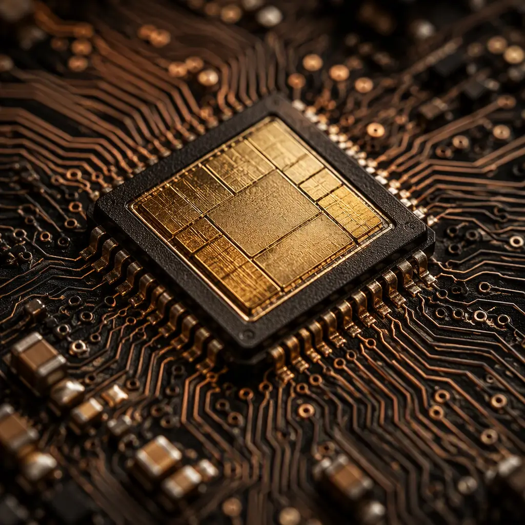
Start With a Threat Model, Not a Shopping List
Hardware security is a cost/risk tradeoff, and the right level depends on what the device protects and who might attack it. A $4 smart plug and a $400 payment terminal have completely different security requirements — and should have completely different boards. Our payment terminal PCB guide covers the PCI PTS tier; here is the general framework.
Define the Asset and the Attackers
What is the crown jewel: the device's private key, customer data in flash, the firmware itself, or the ability to impersonate the device on a network? Who attacks: opportunistic thieves, competitors reverse-engineering your design, or sophisticated adversaries with lab equipment? The answers set the security tier — a casual attacker is stopped by a locked debug port; a professional one requires a tamper mesh and a secure element.
Enumerate the Physical Attack Vectors on the PCB
Every board has a fixed set of physical surfaces: the debug interface (JTAG/SWD), the firmware storage (external flash, MCU internal flash), the communication buses between the MCU and peripherals (I2C, SPI), the power and ground rails, and the bare board surface itself. A threat model maps each asset to the attack paths that reach it — then the design work is closing those paths one by one.
Match the Security Tier to the Product's Value
A useful four-tier scale: (1) consumer devices — read-protected MCU flash and a locked debug port; (2) commercial IoT — add a secure element for device identity and encrypted firmware updates; (3) high-value infrastructure — add tamper detection, encrypted storage, and secure boot with attestation; (4) regulated payment — full PCI PTS with tamper-responsive mesh and certified secure elements. Most B2B IoT products live in tiers 2-3.
Key Takeaway: Security is a tiered design decision, not a component. Decide what the device protects and who attacks it first — then choose the hardware measures that close the actual attack paths.
Secure Elements: Where the Keys Actually Live
A secure element (SE) is a tamper-resistant chip that stores keys and performs cryptographic operations without ever exposing the key material — the MCU asks the SE to sign or decrypt, and the key never leaves the SE's internal storage. Common parts include the Microchip ATECC608/ATECC608B, NXP SE050/SE051, and Infineon OPTIGA Trust series. Our IoT PCB design guide covers the general architecture; here are the security-relevant layout rules.
Route the SE Bus Directly to the MCU, Short and Un-Tapped
The SE communicates over I2C (ATECC608, SE050) or SPI, and that bus is the attacker's primary interception point — a logic analyzer clipped onto the I2C lines can observe key-handling traffic. Keep the SE-to-MCU trace short (under 30 mm), on an inner layer if possible, and route it with no test points, no vias to exposed layers, and no stubs. A series resistor near the SE acts as a current-limiting barrier for probing attempts.
Keep SE Supply and Reset Pins Clean
The SE's VCC needs solid decoupling (0.1 µF plus 1 µF) right at the pin, and the reset pin should be pulled up through a resistor so a glitch attack cannot force the SE into a reset loop during a transaction. Many SEs also expose a tamper input (e.g., the ATECC608's internal tamper detection, or external tamper pins on the NXP parts) — wire these to the tamper detection circuit described below.
Provision Keys at Manufacturing Time, Never in the Field
A secure element is only as good as the provisioning process. Keys should be generated or injected in the factory — ideally inside the SE itself (the SE generates its own key pair and exports only the public part), or loaded through a secure provisioning service from the vendor. This is a manufacturing-process decision as much as a layout one; see the provisioning section below for what to require from your CM.
Secure Boot: The Chain That Refuses Compromised Firmware
Secure boot verifies that the firmware running on the MCU is authentic and unmodified, using a root of trust anchored in hardware. Without it, an attacker who can replace the flash contents owns the device.
Use an MCU With a Hardware Root of Trust and Lockable Debug
Modern MCUs (STM32H7, i.MX RT, nRF5340, and the security-focused Cortex-M33/M55 parts) implement secure boot in ROM, with eFuses or OTP memory that permanently locks the debug port and disables boot from external memory once the production image is committed. The layout side of this is trivial — the security lives in the device configuration — but the board must bring out the right configuration pins (BOOT strapping) with pull resistors that the production process can set and then isolate.
Design the Boot Straps for One-Way Locking
Route BOOT0/BOOT1 straps to a test pad or 0 Ω option rather than a user-accessible jumper, so the production line can configure them and the final unit has no boot-mode switch left open. The debug interface (SWD/JTAG) pads should be present for production testing but buried under components or on an inner layer after finalization — a locked debug port is only locked if there is no exposed port to attack.
Verify, Sign, and Version Every Firmware Update
Secure boot alone does not protect the update path: the bootloader must verify the signature of each new image against the public key stored in the secure element or OTP, and reject downgrades. Board design supports this by giving the MCU a dedicated secure channel to the SE (covered above) and by keeping the update firmware small enough to verify in RAM before committing to flash.
| Security Measure | Stops | Board Design Requirement |
|---|---|---|
| Secure element (ATECC608/SE050) | Key extraction, cloning | Short un-tapped bus, clean supply |
| Secure boot + locked debug | Firmware substitution | One-way boot straps, buried SWD pads |
| Read-protected flash | Dumping via debug | OTP configuration, no exposed test pads |
| Tamper mesh / sensors | Physical intrusion | Fine-pitch mesh, tamper domain battery |
| Encrypted external storage | Chip-off flash reads | Keys in SE, never in external flash |
Tamper Detection: Making Physical Intrusion Visible
For high-value devices — payment terminals, smart meters, access controllers — the board must detect physical intrusion and respond (wipe keys, log the event, alarm). This is where PCB layout becomes a security component in its own right.
Route a Tamper Mesh Over the Sensitive Components
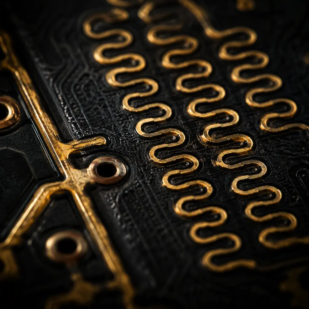
A tamper mesh is a fine serpentine trace (0.1-0.2 mm wide, 0.15-0.3 mm pitch) routed over the top of the board — or on an internal layer pair — covering the MCU, secure element, and flash. The trace carries a continuously monitored signal; drilling, scraping, or probing that breaks or shorts the trace triggers the tamper response. The mesh typically sits on the outer layer with the components on the other side, or as a buried pattern over the IC area. Our 3/3 mil fine-line capability is what makes a genuinely fine mesh practical.
Combine the Mesh With Switch and Sensor Inputs
A complete tamper domain adds: (a) a tamper switch that opens when the enclosure is opened (a PCB edge switch or a conductive pad pair under the cover), (b) optional light or motion sensors inside the enclosure, and (c) the SE's tamper input pin. Wire all of these into a single monitored domain so any single event — cover removal, drilling, light entering the enclosure — triggers the same response.
Power the Tamper Domain From a Battery-Backed Rail
Tamper detection must keep working when the device is unplugged, so the tamper domain (SE + tamper logic + a real-time clock) runs from a coin cell or supercapacitor. The battery sits in its own always-on power rail with a diode to prevent back-feeding, and the tamper response path — SE key zeroization or a tamper latch — must be testable at production. A battery-backed tamper domain is standard on smart meters; our smart meter PCB guide shows it in context.
Anti-Probing Layout: Making the Board Hostile to Analysis
Beyond tamper response, the layout itself can raise the cost of every common attack: bus tapping, chip-off analysis, and fault injection.
Route Sensitive Buses on Inner Layers, Never on the Surface
Signals that carry key material or firmware — the SE bus, the flash bus, and the MCU's debug lines — should be routed on internal layers between two solid ground planes, so they are invisible from the surface and mechanically protected by the board material. Avoid vias that break to outer layers; if a via must rise, keep it under a component footprint.
Hide Test Points and Label Nothing Revealing
Do not put silkscreen labels like "JTAG", "KEY", or "FLASH" on a security board — labeling is an invitation. Test points for production should be covered by solder mask and populated components after test, or use edge-connector test pads that are cut off at depanelization. The silkscreen should describe the board to a technician, not to an attacker.
Encrypt External Storage and Keep the Key Out of Flash
If the design needs external flash (for firmware images or logs), the data should be encrypted with a key that lives only in the secure element — never a key stored in the same flash, and never a hardcoded key in firmware. A chip-off attacker who reads the flash directly should get ciphertext only. This is the single most important rule for devices that hold customer data.
Key Takeaway: Anti-probing design is about cost and friction: every sensitive signal hidden on an inner layer, every test pad buried, every label removed, and every stored byte encrypted raises the attacker's cost above the value of the target.

Manufacturing and Provisioning Security
Hardware security fails at the factory more often than at the attacker's bench. Key material must be provisioned, tracked, and protected through the manufacturing process — which is a contract requirement as much as a technical one. Our IP protection guide and traceability guide cover the commercial side; here is the technical checklist.
Require In-Factory Key Provisioning With a Clean Room Process
Key injection should happen on a dedicated provisioning station with controlled access, logged operators, and no network exposure of the master keys. Prefer SEs that generate keys internally (the private key never exists outside the chip); if keys must be imported, use the vendor's secure provisioning service (Microchip, NXP, and Infineon all offer them) so the CM never handles raw key material.
Program, Lock, and Verify in One Pass
The production firmware flash step should include: program the image, write the OTP/eFuse configuration that locks the debug port and enables secure boot, then verify the boot chain — power cycle the unit and confirm it boots from the locked configuration. A unit that leaves the line without its OTP fuses blown is a unit with an open back door. Huaxing's IC programming service supports this one-pass flow — see our IC programming guide for the details.
Serialization and Chain-of-Custody for Security Boards
Every security board should carry a unique serial number (laser-marked or in the SE certificate), with records linking the serial to the provisioning logs and the final product. This makes a compromised unit traceable to its production batch and supports certificate management. Combined with counterfeit-resistant marking, it also protects your brand — our counterfeit detection guide explains the supply-chain side.
Summary: The Secure IoT Board Checklist
A security-hardened IoT board starts from a threat model, stores keys in a secure element on a short un-tapped bus, boots through a hardware-rooted secure chain with one-way locked debug, protects sensitive signals on inner layers with no revealing labels, adds a battery-backed tamper domain with a fine mesh for high-value designs, encrypts anything stored outside the SE, and is provisioned, locked, and serialized in a controlled factory process. Every one of those measures is a board-level decision — which is why hardware security belongs in the PCB design review, not just the software architecture.
At Huaxing PCBA we manufacture security-sensitive boards up to 32 layers with 3/3 mil fine-line routing for tamper meshes, controlled processes for key provisioning and OTP locking, X-ray inspection, and full functional test including secure-boot verification. Our DFM review checks your tamper mesh geometry, inner-layer routing, and provisioning requirements before tooling. Read our payment terminal security guide for the PCI PTS tier, or send your files for a free DFM review and quote.
