
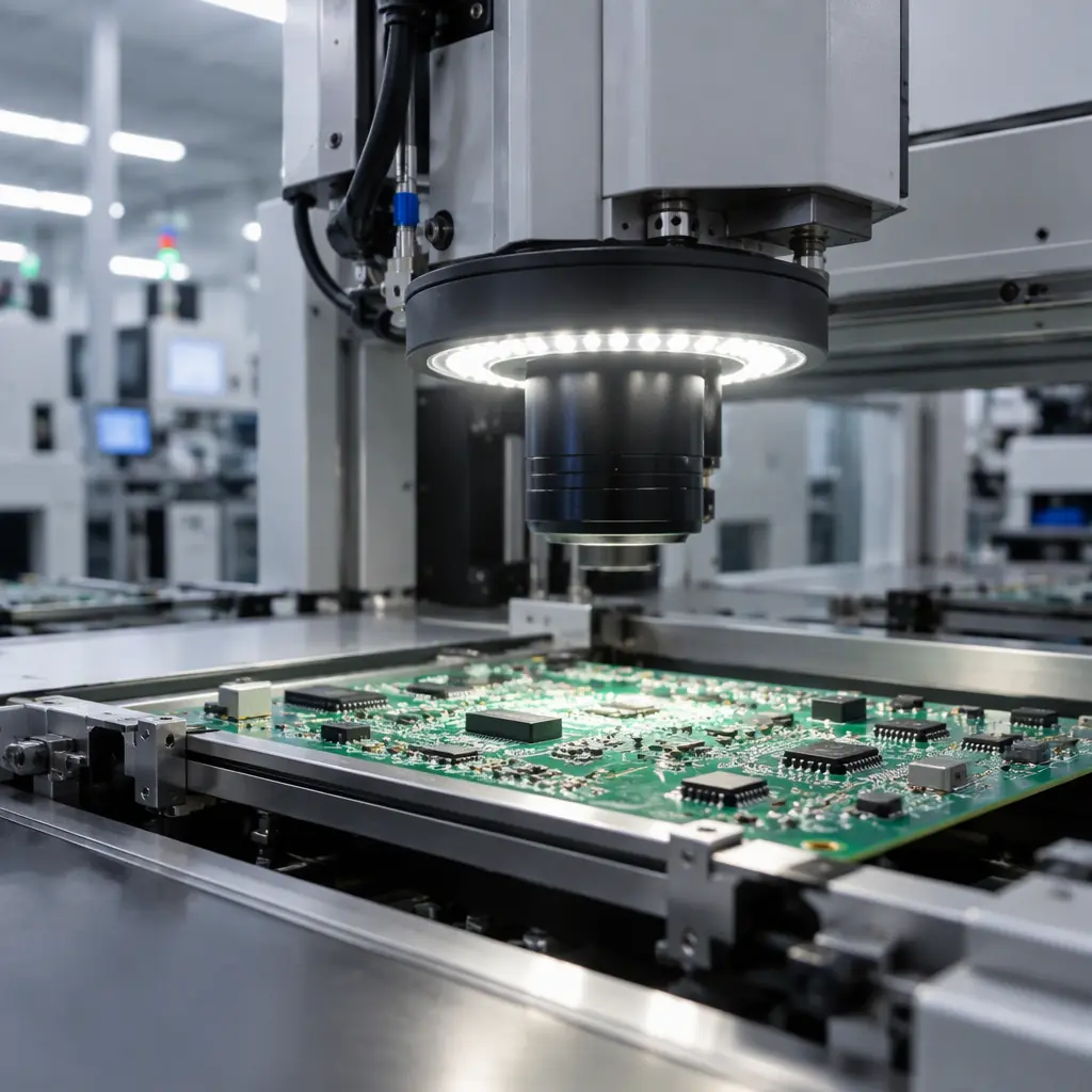
A PCBA test strategy is the answer to a single question asked at several stages of the line: how much evidence do you need, before shipping, that this board is electrically and functionally correct? Every test you add costs money per board and per programme, and every test you omit transfers the cost of a defect from the factory to your customer. A test strategy is the deliberate placement of that cost. When it is done well, the line catches the defects that would have hurt and ignores the ones that would not have. When it is done badly, the same money is spent on tests that pass everything and catch nothing.
This guide covers the four primary PCBA test methods and what each one actually finds, how to choose between them for a given product, how to set a coverage target against your escape cost, and how to place the tests in the order that catches defects at the cheapest possible stage. At Huaxing PCBA we run AOI, x-ray, ICT, flying probe and functional test across 8 SMT lines under IATF 16949 and ISO 9001, and we work with customers to set the test plan at the quotation stage rather than defaulting to whatever the line happens to run.
The Four Test Methods and What Each Finds
The methods are not interchangeable, and understanding what each one is blind to is the core of building a strategy.
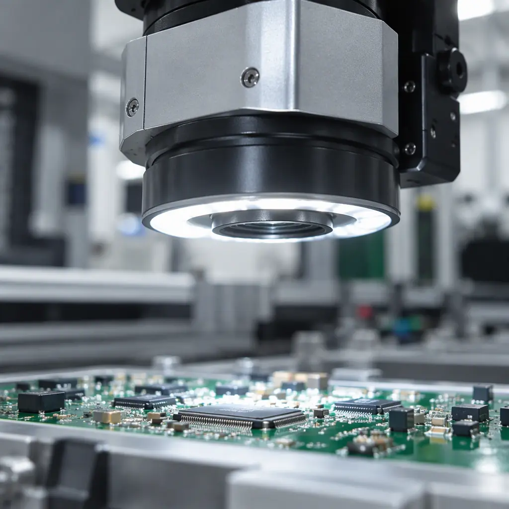
Automated optical inspection (AOI). Vision systems inspect solder joints, component presence, polarity, and placement before and after reflow. AOI is fast, is applied to every board, and excels at catching the placement and solder-shape defects that dominate early production. Its blind spot is hidden joints: it cannot see under a BGA, and it cannot tell whether a joint that looks correct is electrically connected. AOI is the cheapest per-board test and belongs on almost every SMT line.
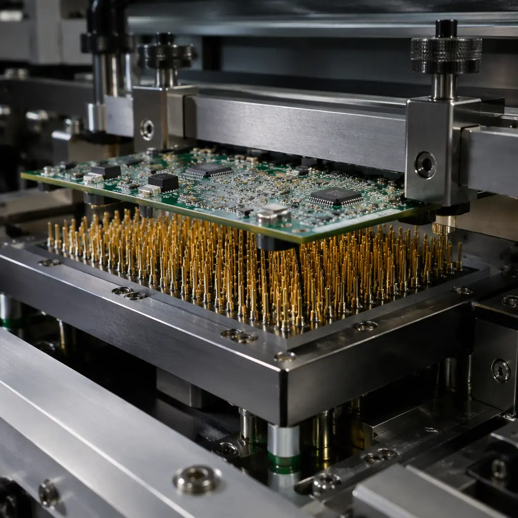
In-circuit test (ICT). A bed-of-nails fixture contacts test points on the board and measures component values, continuity, and shorts. ICT is thorough on assemblies with good test-point access, gives a precise fault location, and is fast per board once the fixture exists. Its costs are the fixture — a significant one-time tooling expense — and the requirement for test-point access, which can conflict with high-density layouts. ICT does not test the board under power with real signals, so it verifies assembly, not function.
Flying probe test. The same electrical measurements as ICT, but delivered by moving probes instead of a fixed fixture. No fixture cost, so flying probe is the natural choice for low and medium volume and for prototypes, and it can reach some points a fixture cannot. The trade is speed: probing is serial, so per-board time is much higher than ICT, and it becomes uneconomic at high volume where a fixture amortises quickly.
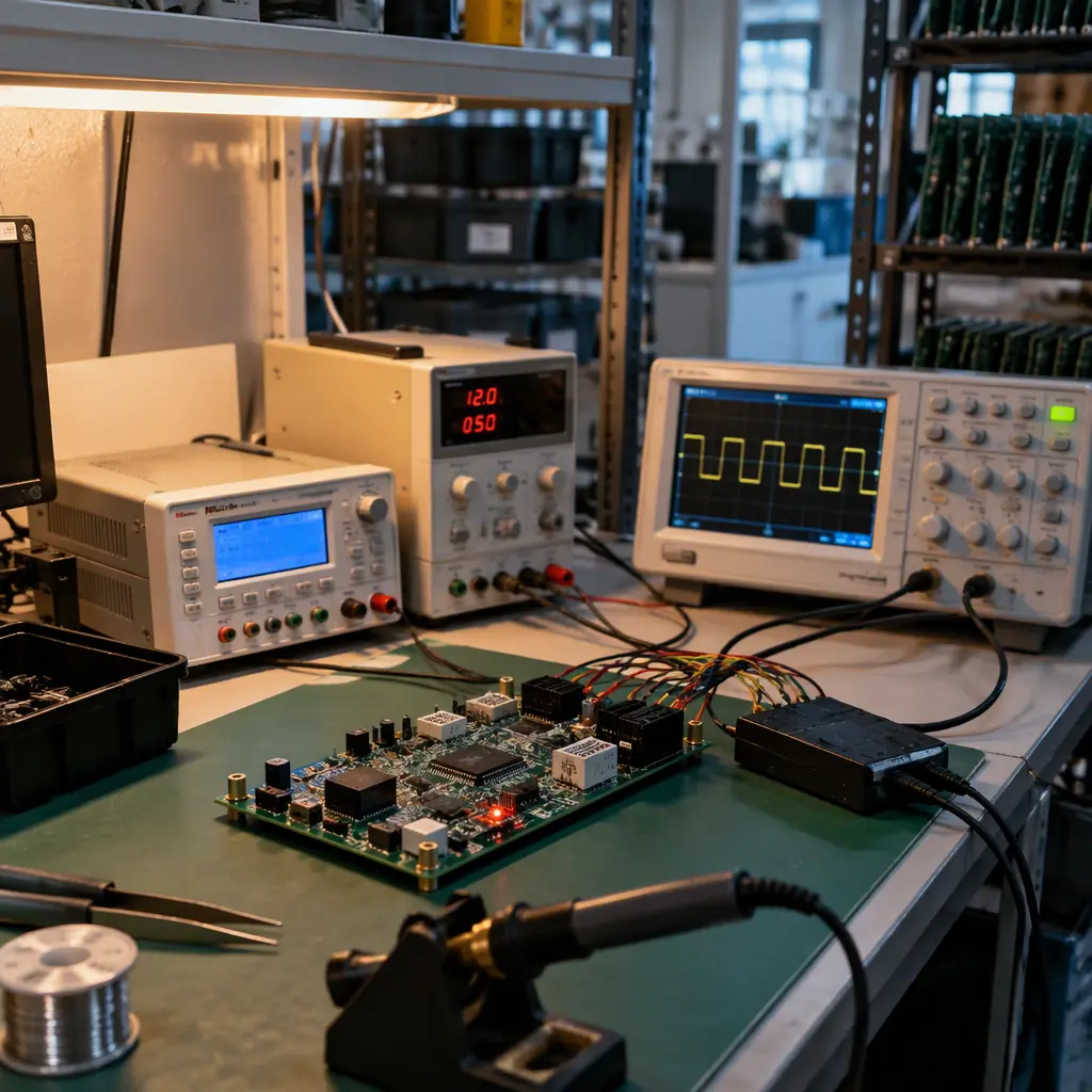
Functional test (FCT). The board is powered and exercised with real or simulated inputs to confirm it does what it is designed to do. FCT is the only method that verifies performance rather than assembly, and it is the closest proxy for the customer's own acceptance test. It requires a test programme, often a custom fixture or bed, and a test specification, and it is typically slower and more expensive per board than the structural tests.
| Method | Finds | Blind To | Best Volume |
|---|---|---|---|
| AOI | Placement, polarity, solder shape | Hidden joints, electrical opens | All volumes |
| ICT | Component values, shorts, continuity | Function, hidden-node access limits | Medium to high |
| Flying probe | Same electrical faults as ICT | Function, serial probing is slow | Low to medium, prototypes |
| Functional test | Real performance under power | Root cause of a fault; slow, costly | All volumes, product-dependent |
Key Takeaway: Structural tests — AOI, ICT, flying probe — prove the board was assembled correctly. Only functional test proves the board works. A strategy that runs only structural tests is verifying the factory, not the product, and will ship boards that are perfectly built and functionally wrong.
Choosing Between ICT and Flying Probe
The most common first decision is ICT versus flying probe, and it resolves almost entirely on volume. ICT carries a fixture cost — a bed-of-nails fixture is a one-time tooling expense, often in the thousands of dollars — and the per-board cost is then low because probing is parallel. Flying probe has no fixture cost and a higher per-board cost because probing is serial.
The consequence is a crossover point. Below a certain cumulative volume, the amortised fixture cost of ICT exceeds the extra per-board cost of flying probe, and flying probe is cheaper. Above it, the fixture is amortised and ICT wins on every subsequent board. A production programme that starts at low volume and scales should usually begin on flying probe and move to ICT once the volume justifies the fixture; committing to a fixture before the volume is known is the classic way to spend tooling budget on a product that never reaches the volume it was sized for.
Test-point access complicates the choice. ICT needs enough test points to reach every net, and dense designs with no room for large test pads may not be fixture-able. In that case flying probe, which can probe smaller and differently located points, may be the only structural option — which is why access should be designed in from the start, not discovered at test. The trade between the two is examined in more detail in our flying probe vs ICT vs functional test guide.
Setting a Coverage Target Against Escape Cost
Coverage — the fraction of possible faults your test plan can detect — should be set by what an escape costs, not by what feels thorough. A board that goes into a consumer toy and a board that goes into a medical monitor carry very different consequences for the same escaped defect, and their test plans should differ accordingly.
The calculation is to compare the cost of testing against the cost of an escape. If a defective board costs E to handle in the field — including returns, rework, freight, reputation, and for regulated products the possibility of recall — and a test that would have caught it costs T per board, then adding the test is worthwhile whenever the escape rate times the escape cost exceeds the added test cost. A structural test costing a few cents per board removing a defect that would cost hundreds in the field is an easy yes. A test costing several dollars per board to catch a defect that would cost the same to fix on the line is not.
The practical rules that follow are consistent across products:
Always run AOI — it is the cheapest coverage per board
AOI catches the high-frequency placement and solder defects at a per-board cost far below the alternatives. There are few products where omitting it makes sense.
Add electrical test where escape cost is high or access permits
When a field escape is expensive, the structural electrical test that catches shorts and wrong values pays for itself easily — provided the design offers the test-point access to run it.
Run functional test on every product that has a function to verify
Where the board does something — powers up, communicates, measures, drives — a functional test is the only way to prove it works. Its cost is justified by the faults it catches that no structural test can see.
Match sample testing to process stability
For a stable, high-volume process, sampling or periodic testing can replace 100% test on the dimensions that are demonstrably under control, reducing cost without increasing escape risk. For unstable or new processes, keep 100% until the data supports reducing it.
Placing the Tests in the Right Order
The order in which tests run determines what each one costs, because a defect caught early costs less to fix than the same defect caught late. The general principle is to catch a defect at the cheapest stage that can detect it.
Solder paste inspection (SPI) sits first, before reflow, and catches paste-volume problems that would otherwise become solder defects downstream. AOI after reflow then catches placement and solder-shape faults. Electrical structural test (ICT or flying probe) follows, catching shorts and value faults that vision cannot see. Functional test comes last, on a board that has already passed every structural gate, so that a functional failure is more likely to be a real design or component issue than a masked assembly defect. This ordering is what our guide to AOI, X-ray and SPI inspection describes from the inspection side, and the cost structure of the fixtures involved is covered in ICT and FCT fixture cost.
Putting the Strategy on the Order
A test strategy becomes real when it appears on the order as a specification: which tests run, at what coverage, on what sample, with what acceptance criteria, and what happens to a board that fails. Without that, the factory runs its default plan, which may be more or less than the product needs and is not tuned to the escape cost the customer actually faces.
The cleanest way to set it is to state, for each test method, whether it is 100% or sampled, what it is verifying, and the pass criterion. Add the fault-handling rule — rework and retest, or scrap — so the disposition of a failed board is decided in advance. Then review the plan after the first production run against the actual defect data: the tests that caught nothing and the defects that escaped are both evidence about where the plan should change.
At Huaxing PCBA we run AOI, x-ray, ICT, flying probe and functional test across 8 SMT lines under IATF 16949 and ISO 9001, and we set the test plan with the customer at quotation rather than defaulting to the line's standard. Send your Gerber and BOM with your target application and expected volume and we will propose a test plan matched to your escape cost and return a quote inside 24 hours, or talk to our engineering team about the right test coverage for your product.
