
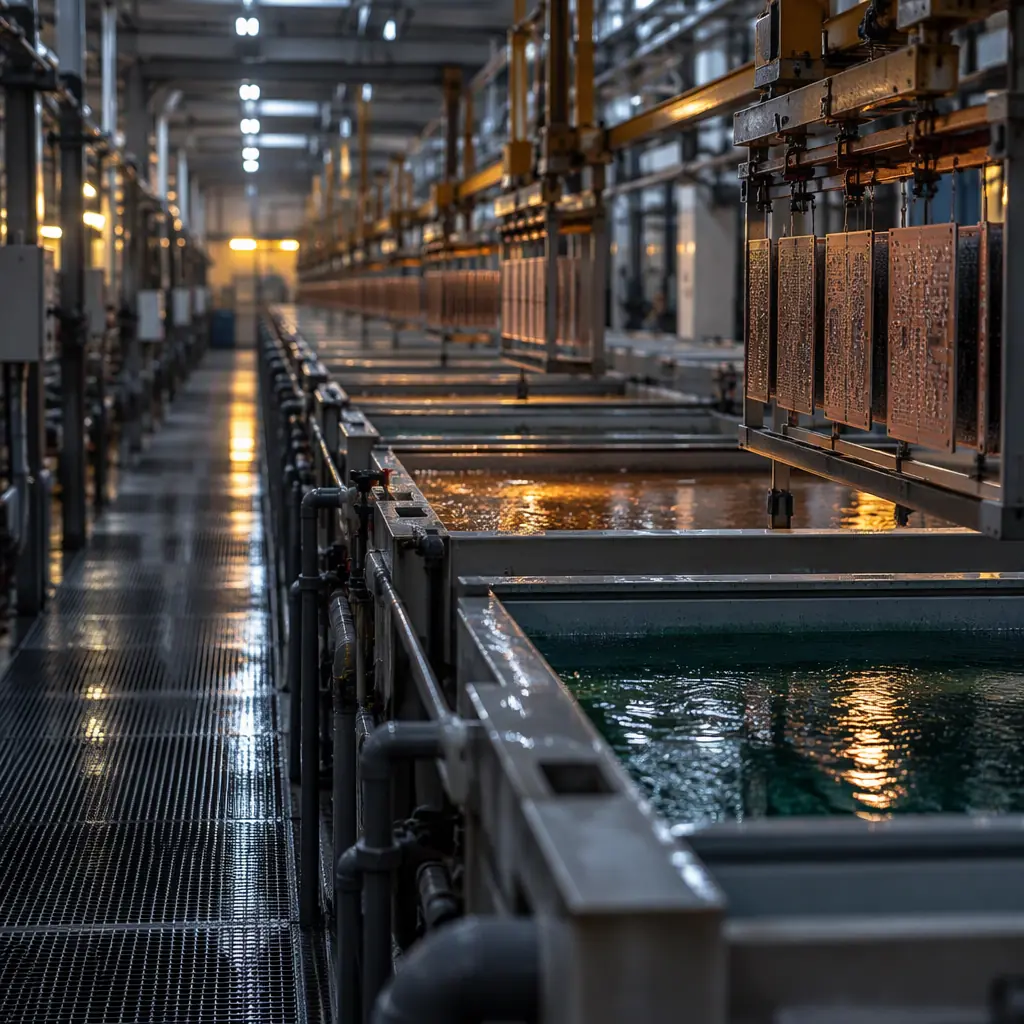
A question that used to sit in the annual report has moved into the RFQ. Procurement teams — particularly those supplying European OEMs or listed customers — are now asked to collect product carbon footprint data from their PCB supplier before award, not after. The problem is that most PCB fabricators have never had to produce a defensible number for electricity, water or chemistry per square metre of board, and the response is often either a generic corporate figure lifted from a sustainability page or a modelled estimate presented as if it were measured. This guide is written for the buyer who has to put that number into a report and defend it.
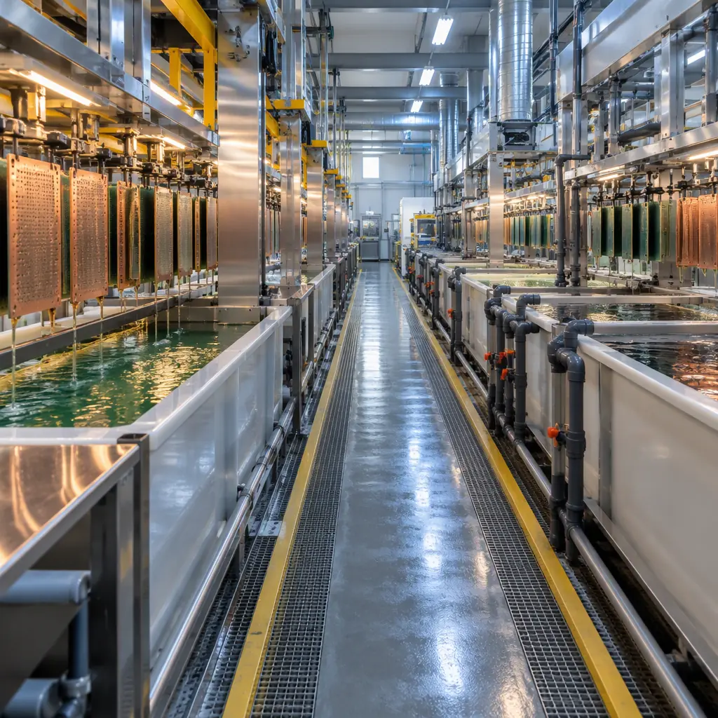
Why PCB Carbon Data Is Now a Procurement Requirement
Three forces converged. The first is the EU Carbon Border Adjustment Mechanism, whose transitional reporting has already required importers of certain goods to declare embedded emissions, with the scope broadening over time. Electronics are not yet the headline category, but the CBAM methodology has set the expectation that upstream suppliers can produce embedded-emission data on request. The second is the Corporate Sustainability Reporting Directive and its spillover: large customers subject to CSRD must report Scope 3 emissions, and a PCB is part of their upstream Scope 3. The third and most immediate force is simply the customer ESG questionnaire, which now routinely asks a supplier for its energy intensity, renewable share and any product-level footprint figure.
The practical effect is that the question arrives early — typically at the RFQ stage, often as a spreadsheet to be completed alongside the quote. A supplier that cannot answer it credibly is increasingly filtered out before commercial evaluation, which is why the capability is now a procurement-relevant one rather than a marketing one.
Where the Carbon Actually Sits in a PCB
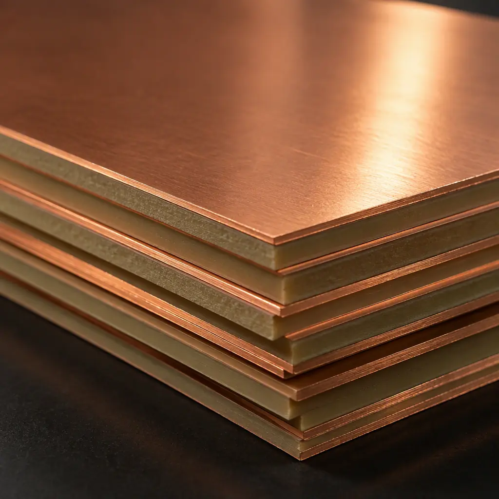
The intuition most buyers bring is that the fabricator's own electricity is the whole story. It is not. For a bare rigid PCB, the majority of the embedded footprint sits upstream, in the materials — chiefly the copper foil and the laminate — rather than in the drilling, plating and imaging steps the fabricator performs. A useful working split for a standard FR-4 multilayer board is that a large majority of the total is upstream materials, with the fabricator's own process energy making up the remainder. The exact split moves with layer count, copper weight and board area, but the direction is consistent and it changes where you should push.
| Process Step | Main Carbon Driver | Lever Available to the Buyer |
|---|---|---|
| Copper foil production | Energy-intensive electro-refining and rolling, upstream of the fab | Use the thinnest copper that meets current and thermal needs — this is the single biggest lever |
| Laminate production | Resin chemistry and curing energy | Specify standard FR-4 where a high-performance material is not required |
| Drilling and routing | Machine electricity per panel, drill count and stack height | Reduce layer count and total hole count at design stage |
| Plating and surface finish | Electricity plus chemistry consumption and waste treatment | Choose a finish appropriate to the application rather than defaulting to the most expensive one |
| Panel utilisation | Fraction of each panel that becomes a usable board | Improve nesting — wasted panel area carries the full footprint of everything upstream |
The last row is where the buyer has the most influence for the least effort. A panel that yields sixty percent usable board against eighty percent carries roughly a third more embedded carbon per finished board, because the upstream material footprint is spent on the whole panel. That is why better panel utilization and nesting is a legitimate carbon reduction action, not just a cost one. The same logic rewards keeping copper weight to what the design genuinely needs rather than over-specifying, which is the subject of the heavy copper decision.
The Numbers a Supplier Can Legitimately Give You
The dividing line between a credible report and a decorative one is whether the numbers are metered or modelled. A fabricator can reasonably meter: electricity consumed per square metre of panel processed, and separately per square metre of finished board; water consumption in cubic metres; waste chemistry volumes; and its own renewable share or grid mix, since China's grid emission factor is published annually and varies by region. Those are measurable against utility bills and meter readings.
What a fabricator generally cannot meter is the upstream footprint of the laminate and copper foil it buys, unless the material supplier provides primary data, which most do not at PCB scale. In that case the upstream portion is modelled from published emission factors and should be labelled as such. That labelling is the whole game: a modelled estimate clearly marked as modelled is honest, whereas the same number presented as measured is a defect waiting to be found. When you receive a footprint figure, ask for the boundary, the emission factor sources with their publication years, and which proportion is primary versus modelled data.
Useful per-unit metrics to standardise on are kilowatt-hours per square metre of finished board and of panel processed, which normalises across panel sizes, plus cubic metres of water per square metre. Agreeing those units up front stops the two sides comparing incomparable numbers, and it makes year-on-year improvement measurable rather than anecdotal.
What a Product Carbon Footprint Report Must Contain
A credible product carbon footprint states the functional unit — for a PCB, usually one square metre of finished board at a defined layer count and copper weight — the system boundary, whether cradle-to-gate or cradle-to-grave, the emission factor sources and their publication years, the allocation method used when one panel produces several boards, the date of the data, and who verified it, if anyone.
Functional unit defined explicitly
One square metre of finished board at a stated layer count, copper weight and thickness. A footprint per panel is meaningless if the panel size is not given.
System boundary declared
Cradle-to-gate covers raw materials through the finished board leaving the factory. If transport is included, say so. If end-of-life is included, say so.
Emission factors cited with year
The electricity emission factor is the single most sensitive input, and it changes annually as the grid decarbonises. A report without a factor year cannot be compared to anything.
Allocation method stated
When one panel yields several boards, or when a line runs several products in a shift, the energy has to be allocated. By area, by panel count or by machine time — the choice changes the answer.
Primary versus modelled split visible
Metered data and modelled data must be distinguishable in the report itself, not explained on request.
Data period and verifier named
A footprint is a snapshot. State the period it covers and whether a third party verified it, and if not, say plainly that it is unverified.
What Is Not Credible — Greenwashing Flags
When a supplier's carbon claim arrives, several patterns should stop the evaluation rather than start it. These are not edge cases; they are common in the PCB tier because the pressure to answer has arrived faster than the capability to measure.
- "Carbon neutral" with no boundary. Neutrality against an unstated scope is unfalsifiable. Ask what is included and what the residual was before offsets.
- Offsets presented as reduction. Buying credits does not reduce the emissions embedded in your boards. A credible supplier reports reduction first and offsets separately, if at all.
- Scope 3 estimates presented as measured. Upstream material emissions are almost always modelled at PCB scale. Presenting them as primary data is the single most common misrepresentation.
- No emission factor year. A figure without a factor year cannot be compared to last year's report, which is usually why it is omitted.
- A corporate figure offered as a product figure. Group-level intensity per revenue or per employee says nothing about the footprint of your board.
- Renewable claims without certificates or contracts. A percentage of renewable electricity should be backed by a certificate, a power purchase agreement, or on-site generation evidence.
Cheap Wins That Genuinely Reduce Footprint
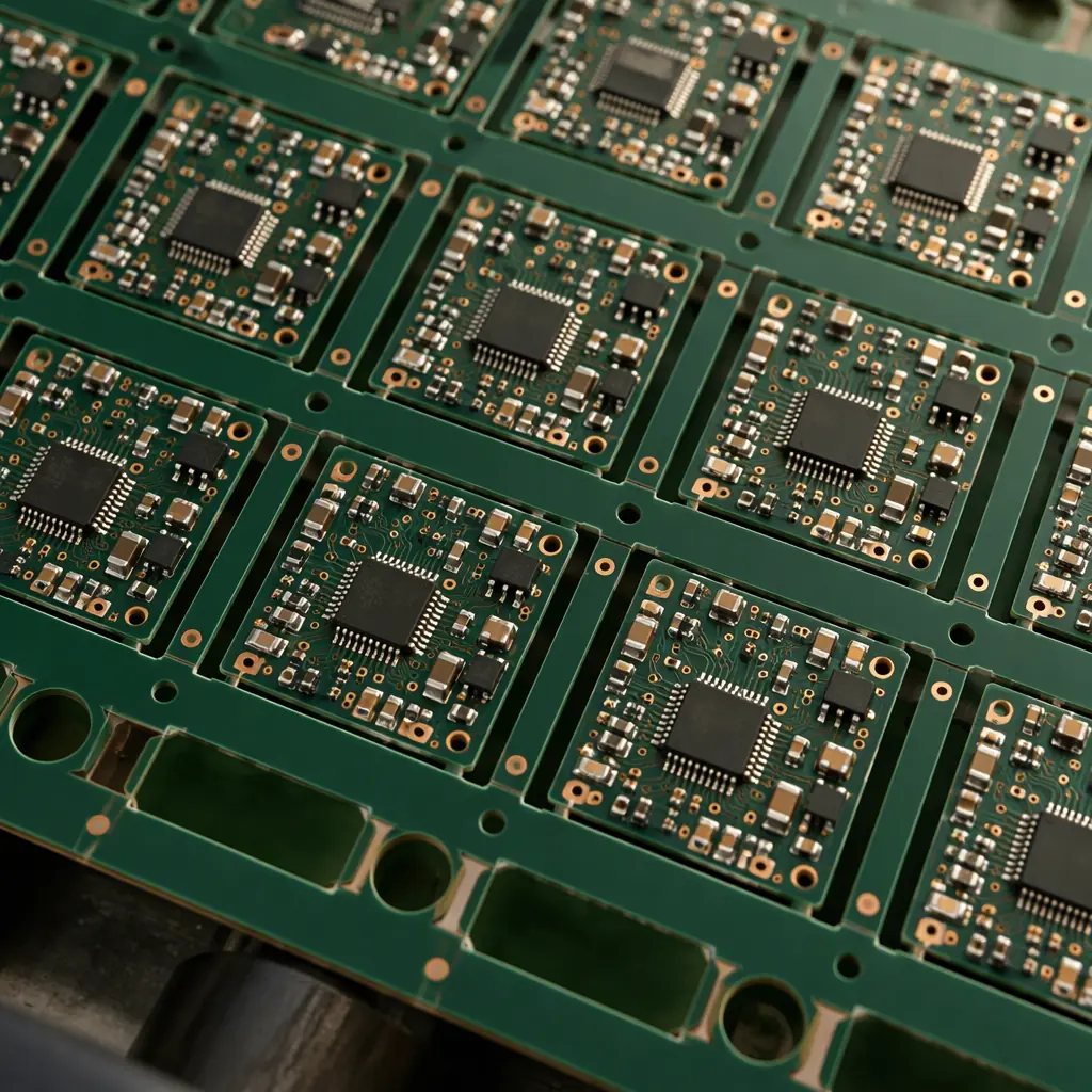
Reduction is more credible than reporting, and several actions reduce embedded carbon while also reducing cost — which is why they are worth pushing for in the RFQ rather than treating as corporate overhead. Improving panel nesting and utilisation reduces the material footprint per finished board directly. Reducing copper weight to what the design needs, and reducing layer count where the electrical and thermal requirements allow, both cut the largest upstream contributors. Cutting rework and scrap reduces the footprint of boards that are built and then discarded. And consolidating freight — shipping complete assemblies rather than board and components separately — removes transport emissions that would otherwise be charged to your product.
None of these require a supplier to install anything. They require the buyer to stop over-specifying and the supplier to report panel utilisation honestly, which is the same discipline that already drives cost in the cost drivers of a board and in the underlying raw material pricing.
At Huaxing PCBA we report energy and water intensity per square metre of finished board from metered fab data, and we label the upstream material portion as modelled against published emission factors with the factor year stated rather than presenting it as measured. Boards are built to IPC-A-610 Class 2 and 3 and to IATF 16949 and ISO 9001 quality systems across 8 SMT lines in Shenzhen. Send your Gerber, BOM and the ESG data format your client requires and we will return the quote with the footprint inputs your report needs, or talk to us about a footprint baseline for an existing program.
