
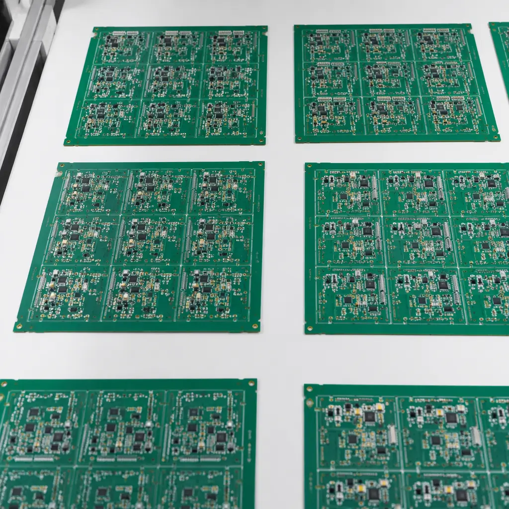
When you request a PCB quote, the manufacturer prices by the panel — not by the individual board. A standard PCB production panel measures 18 × 24 inches (457 × 610 mm), and every square inch you leave as rail, gap, or empty space is square inches you're paying for but not shipping. Panel utilization — the percentage of the panel area occupied by actual PCB units — is the quiet margin-killer in PCB procurement. A design with 65% utilization vs 85% utilization on the same panel costs 30% more per board. Not because the board is more complex. Because you're throwing away one-third of the panel.
At Huaxing PCBA, our CAM engineers run nesting optimization on every order before quoting, but the biggest gains come from decisions made during PCB layout — long before the Gerber files reach us. This guide explains the four variables that determine panel utilization, how to make layout decisions that maximize boards per panel, and when a custom panel size (non-standard 18×24") is worth the tooling investment. We manufacture over 80,000 m² of PCBs monthly — the difference between 70% and 90% utilization over that volume is measured in hectares of saved laminate.
The Four Variables That Determine Boards Per Panel
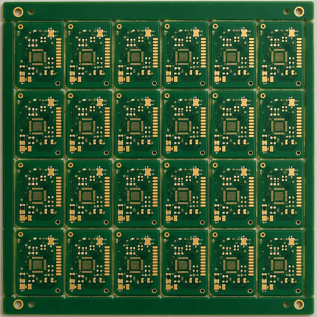
Panel utilization is a geometry problem with four degrees of freedom. Changing any one of them can add or remove entire rows or columns of boards from the panel — and each row on a 18×24" panel represents thousands of dollars at production volume.
| Variable | Typical Range | Impact on Utilization | Who Controls It |
|---|---|---|---|
| Board dimensions (X × Y) | From 10×10mm to 600×800mm | Primary — determines the integer fit into 18×24" | PCB designer / layout engineer |
| Rail width (panel border) | 8mm (tight) to 20mm (generous) | 2-8% per 5mm reduction | Manufacturer (but specifiable) |
| Board-to-board gap | 1.6mm (V-score) to 5mm (tab-route) | 3-6% depending on depanel method | Manufacturer → driven by depanel choice |
| Board rotation (0°/90°) | 0° vs 90° nesting | 0-15% — can be dramatic for rectangular boards | CAM engineer at manufacturer |
The golden rule of panel utilization: The standard panel is 18 × 24 inches. If your board's X and Y dimensions (including the board-to-board gap) divide evenly into 18 and 24, you get near-perfect utilization. If they don't, you pay for the remainder. A board that is 48.5mm wide will fit 9 across a 457mm panel (9 × 48.5 = 436.5mm, leaving 20.5mm for rails and gaps). A board that is 49.0mm wide will still fit 9 — but a board that is 51.0mm wide now fits only 8. That 2.5mm dimension difference costs you 11% of your boards per panel. This is why we recommend you run a panelization check during layout, not after.
Rail Width: The Invisible Cost Driver
The panel rail (also called the frame or border) is the unused perimeter of the panel that provides mechanical rigidity during automated SMT assembly. It hosts tooling holes, fiducial marks, and sometimes test coupons. Every millimeter of rail width is a millimeter of panel space that cannot contain PCB units — and it's applied to all four sides of the panel.
A standard rail width of 15mm on all four sides consumes 15 × (457+610) × 2 = 32,010 mm² — about 11.5% of the 278,770 mm² panel area. Reducing rail width from 15mm to 10mm recovers 10,670 mm², which on a panel yielding 24 boards of 10,000 mm² each, adds one full extra board. At a panel cost of $40, that's $1.67 saved per board — and for an annual volume of 100,000 boards, the saving is $167,000 with zero change to the PCB design.
Rail Width by Assembly Technology — When You Can Go Narrow
Standard SMT (12-15mm rail): Required for conveyor-edge clearance on automated placement machines. This is the safe default for any design.
Narrow rail (8-10mm): Feasible if your board has no edge-mounted connectors within 5mm of the board edge, and the SMT line uses edge-clamping rather than conveyor-belt transport. Discuss with your manufacturer — most can accommodate 10mm rails for standard designs.
Rail-less (0mm on non-conveyor edges): The two edges perpendicular to the conveyor direction can have near-zero rail — only 2-3mm for the V-score clearance groove. This is standard practice for high-volume consumer electronics PCBs where every cent counts. Specify "rail only on conveyor edges" in your fabrication notes.
V-Score vs Tab-Routing: How Depanelization Method Drives Utilization
The method used to separate individual boards from the panel determines the minimum board-to-board gap — and different gaps mean different boards-per-panel counts. The choice isn't purely mechanical; it has a direct financial consequence.
| Depanelization Method | Board-to-Board Gap | Best For | Utilization Impact |
|---|---|---|---|
| V-Score | 0 mm (boards touch, ±0.1mm score line) | Rectangular boards, straight edges | Maximum — no gap wasted |
| Tab-Route with mouse bites | 2.0-3.0mm routing channel | Odd-shaped boards, internal cutouts | Moderate — 2-3mm per row/column lost |
| Tab-Route with full perimeter route | 3.0-5.0mm routing channel | Boards with edge connectors or castellated holes | Significant — up to 8% of panel area lost |
| Laser depaneling (no tabs) | 0.5-1.0mm (laser kerf) | Ultra-thin (0.2-0.5mm) or fragile boards | Near-V-score — minimal gap loss |
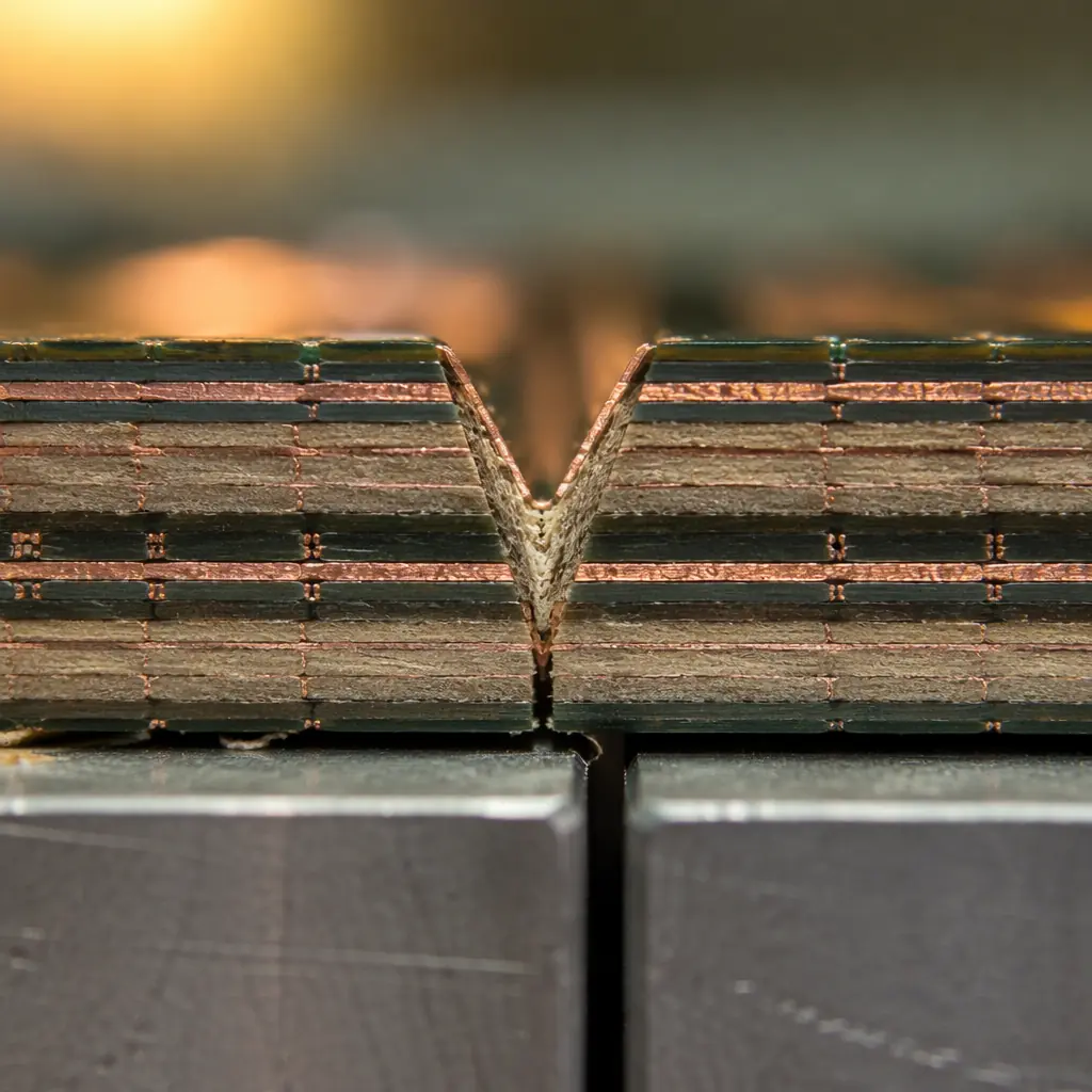
V-score is the utilization champion: boards are fabricated as one contiguous piece with a V-shaped groove cut one-third of the way through from both sides, and they snap apart after assembly. But V-score only works for straight-line edges — you can't V-score a curve, an internal cutout, or a board with castellated half-holes along the edge. For those, tab-routing is necessary, and the 2-3mm routing channel between boards becomes unavoidable dead space. If your design permits V-score (rectangular outline, no edge connectors on the V-score edges), specify it — the zero-gap adjacency typically adds 1-2 extra boards per row compared to tab-routing. Our depaneling methods guide covers the full selection matrix including stress limits for each method.
Mixed-method panels: You can combine V-score on straight edges with tab-routing on irregular sections. A common pattern: V-score the X-axis separation (straight board edges) and tab-route the Y-axis (boards with cutouts on the top/bottom edge). This hybrid approach captures most of V-score's utilization advantage while handling non-rectangular outlines. Discuss with your CAM engineer during the quote review process.
Mixed-Panel Strategy: When to Nest Two Different Designs Together
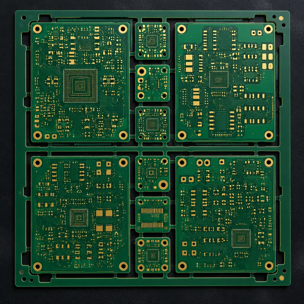
If your product has two PCBs — say, a main board (45 × 60mm) and a small connector board (15 × 20mm) — putting them on separate panels means each panel carries only one design. The small board's panel utilization will be terrible: a 15×20mm board is tiny compared to a 457×610mm panel, and even with optimal nesting, you might only reach 50-60% utilization. The better approach: nest both designs on the same panel.
A mixed panel fills the gaps that would otherwise be dead space. The main boards are laid out in a regular grid, and the small connector boards fill the remaining rectangles between them. The result: combined utilization can reach 85-92%, where separate panels might achieve 80% and 55% respectively. The constraint: both designs must use the same laminate material, copper weight, layer count, and surface finish — and both must be ordered in the same quantity ratio. If you need 1,000 main boards and 500 connector boards, a mixed panel can produce them in exact proportion (e.g., 4 main + 2 connector per panel, 250 panels total).
The cost math is compelling. Assume a standard 4-layer panel costs $42. With separate panels: main board at 80% utilization = 72 boards/panel = $0.58/board; connector board at 55% utilization = 850 boards/panel = $0.05/board. With a mixed panel at 88% utilization: 64 main + 32 connector per panel = $0.44/main + $0.04/connector. The saving is $0.14/main board. At 100,000 main boards/year, that's $14,000 — for a change that requires no redesign, only a different panelization instruction. For more on the economics of production scaling, see our prototype vs production cost breakdown.
Custom Panel Sizes: When to Break the 18×24″ Rule
The standard 18×24″ panel exists because laminate manufacturers produce sheets in 36×48″ and 40×48″ formats that are cut into four 18×24″ or four 20×24″ panels. But if your board dimensions result in poor utilization on 18×24″, a custom panel size can be worth the tooling investment — especially at production volumes above 10,000 units.
Example: Your board is 52 × 78mm. On 18×24″ (457×610mm) with 12mm rails and V-score: you fit 7 × 7 = 49 boards, utilization = 74%. On a custom 16×22″ (406×559mm) panel: you still fit 7 × 7 = 49 boards, but the panel costs 18% less because it's smaller. OR: on a custom 20×26″ (508×660mm) cut from a 40×52″ laminate sheet: you fit 9 × 8 = 72 boards at 81% utilization — that's 47% more boards per panel, and the panel cost only increases by 32%. The net per-board cost drops by ~10%. The break-even on the custom panel tooling fee (typically $200-500) is usually under 1,000 units.
Ask your PCB supplier: "What panel size gives the best boards-per-panel yield for our board dimensions?" A good CAM engineer can run this optimization in under 30 seconds — the nesting algorithm tries every standard and semi-standard panel dimension and reports the highest yield. Most buyers never ask this question, and they leave 10-15% on the table. For guidance on evaluating supplier capabilities, see our PCB supplier audit checklist and our comprehensive cost factors guide.
The Panelization Checklist for Maximum Utilization
Before you send Gerber files to your PCB manufacturer, run through this checklist. Each "yes" answer adds boards per panel and subtracts cost per board.
Board dimensions: Is either X or Y a multiple of the panel dimension minus rails?
Target: (board_dimension + gap) × N ≈ (457mm − 2 × rail_width). For 10mm rails, that's 437mm usable. If your board+gap is 48mm, you fit 9 across (432mm) with 5mm spare. If it's 50mm, you fit 8 (400mm) with 37mm wasted. That 2mm decision during layout is worth 12.5% more boards. Run this calculation during PCB layout — not after the design is frozen.
Can you use V-score instead of tab-routing for at least two edges?
V-score eliminates the 2-3mm routing channel between boards, adding 1-2 extra boards per row. Check: are all four board edges straight? Are there no edge connectors or castellated holes on the X-axis edges? If yes to both, specify V-score on the straight edges. Even partial V-score (two edges V-score, two edges tab-route) improves utilization vs full tab-routing.
Can rail width be reduced from 15mm to 10mm on non-conveyor edges?
Confirm with your assembler that their SMT line supports 10mm rails and that no edge-mounted components are within 5mm of the board edge. If confirmed, specify "10mm rails on conveyor edges, 8mm rails on non-conveyor edges." The 5mm reduction on two edges recovers ~5,350 mm² — enough for half a board on many designs.
Do you have two or more PCB designs using the same stackup?
If yes, ask your manufacturer to quote a mixed panel. The utilization gain from filling gaps with a second design is typically 5-12 percentage points. This is especially powerful when one board is much smaller than the other — the small board acts as a "gap filler" that would otherwise be dead laminate. See our panelization cost optimization guide for mixed-panel design rules.
The ROI: What 10% Better Utilization Is Worth
Let's put real numbers on it. A medium-complexity 4-layer PCB (100×80mm, ENIG, green solder mask) in 10,000-unit annual volume. At 75% panel utilization: 42 boards per 18×24″ panel, panel cost $38, per-board cost $0.90. At 85% utilization (achievable with V-score + 10mm rails + board dimension optimization): 48 boards per panel, panel cost $38, per-board cost $0.79. Annual saving: $1,100. That pays for the engineering time to run the optimization 10 times over. At 100,000 units: saving is $11,000. For high-layer-count boards ($120/panel), the absolute saving is 3-4× larger.
The best part: none of these optimizations require changing the PCB's electrical design. The schematic, layout, component placement, and routing all stay exactly the same. Panel utilization is a manufacturing optimization that pays for itself in the first production run — and keeps paying on every reorder. For buyers managing PCB supply chain costs, it's the highest-ROI cost reduction lever available.
Send us your board outline — we'll run the nesting optimization and return a panel utilization report with cost at 3 utilization levels, within 24 hours. No charge, no commitment. Just math.
