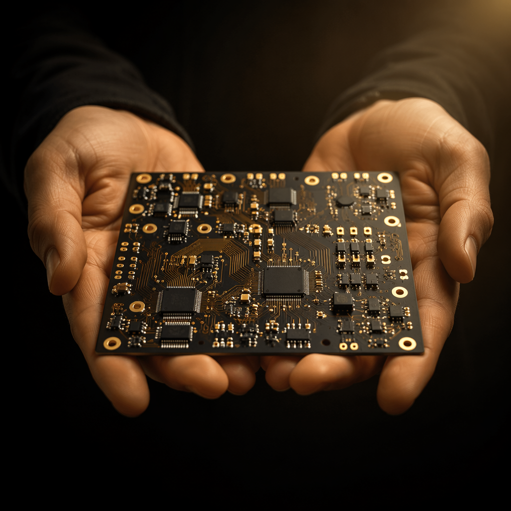

A loose 0402 capacitor inside a sealed enclosure is not a cosmetic defect. It is a delayed short circuit, and it usually closes its circuit on a customer site, at a temperature cycling extreme, after the unit has passed final test and shipped. That is the defining problem with foreign object debris on an assembly line: the debris is invisible at the moment of manufacture, the inspection gate that would catch it is not always installed, and the failure it produces arrives months later with no traceback to the line that released it.
Foreign object debris control, FOD in the aerospace vocabulary, is treated as a formal programme in AS9100 environments and as housekeeping in most commercial ones. The gap between those two positions is where the expensive escapes live. This page sets out where FOD on a printed circuit board assembly actually originates, which detection method catches which type of debris and what each costs, and the clause language that puts the liability for an escape where it belongs before an order is placed. It is written for buyers and quality engineers who are specifying assembly work rather than running the line, and it assumes the reader already knows how to buy a board. The inspection stack that surrounds this problem is covered in AOI, X-ray and SPI inspection guide; this page is about the material that arrives on the board from somewhere other than the bill of materials.
Why FOD Survives to Pack-Out
Debris does not appear at random. It enters a build at a finite number of points and survives to pack-out through a finite number of mechanisms, and both sets are short. Understanding them is what makes a control plan checkable rather than aspirational.
The assembly environment is a low-margin, high-speed process. Boards move on conveyors, carriers and magazines; components arrive in tape, trays and tubes; the process uses paper, plastic and metal in direct contact with the product. Every one of those contacts can shed material, and the material that sheds is often the exact size that fits under a shield can, inside a connector shroud, or beneath a fine-pitch BGA where no camera can see it.
The second half of the mechanism is concealment. Debris that remains visible at the AOI gate is a found defect and costs a rework touch. Debris that ends up under a component, inside an overmould, or behind a shield is a latent defect, and latent defects are the only ones with a field-return cost attached. A control plan that only measures visible debris is measuring the cheap half of the problem.
The Source Table
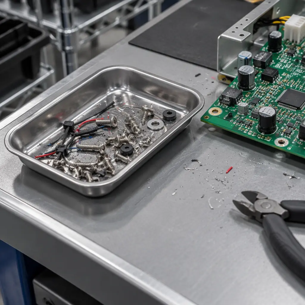
Manual operations at the assembly station introduce the largest debris in the whole process: fastener ends, wire trims and tape backing.
The table below is the practical core of this page. It lists the six sources that account for most FOD in a PCBA build, the typical size of the debris each produces, the path by which it survives to pack-out, and the detection method that will actually see it.
| Source | Typical debris and size | Escape path | Detection that catches it |
|---|---|---|---|
| Solder ball generation during reflow | Spheres 0.1 to 0.5 mm | Stays on board surface, hides under low-clearance parts; migrates into cavity after vibration | 5-axis X-ray; AOI if on a visible surface |
| Tape and reel carrier debris | Cover-tape fragments, pocket lining flakes, 0.2 to 2 mm | Dropped into the placement area when a reel splice is made; lands on unpopulated pads | AOI after placement; pre-reflow visual at load |
| Component carrier and tray foam | Foam crumbs, tray lining dust, 0.1 to 1 mm | Clings to part bodies by static; released inside the machine | Post-placement AOI; incomplete without cleaning |
| Manual insertion and hand-solder | Solder wire ends, insulation trims, wire strands, 1 to 5 mm | Left in the work area; falls into open housings during box-build | Box-build line clearance audit; not visible to PCB-level AOI |
| Depanel debris | Fibreglass dust, copper slivers from routing and V-scoring, 0.05 to 1 mm | Coating the board edge and migrating inward during handling | Post-depanel cleaning verification |
| Packaging and transit | Desiccant beads, bag liner flakes, cardboard dust | Present before the bag is sealed; introduced at pack-out | Pack-out line discipline; X-ray before bag seal |
Two entries in that table deserve emphasis because they break the usual assumption that AOI is the last line of defence. Manual insertion debris and packaging debris both occur downstream of the PCB-level inspection gate, so on a box-build or a fully assembled unit the PCB inspection stack has already closed before the debris enters. A programme that only inspects at the board level has no detection coverage for two of the six sources, and those two are the ones with the largest debris and the highest probability of bridging a power rail.
What the Standards Require and What They Do Not
Buyers often assume "no foreign material" is an acceptance criterion they can point to. It is not, at least not in the form they expect.
IPC-A-610 treats foreign material as a condition that must be evaluated for its effect rather than as a binary failure. The question the standard asks is whether the material reduces electrical clearance, whether it is conductive, whether it is loose, and whether it is in a position to migrate. That framing is more useful than a blanket prohibition because it distinguishes a fibreglass dust particle on a solder mask from a loose copper sliver bridging a 0.5 mm gap, and a supplier can legitimately argue the first is acceptable while having no defence on the second.
elevates FOD to a programme requirement. The aerospace standard, in its risk and product realisation clauses, expects a documented FOD prevention programme, control of tools and loose articles, defined FOD prevention areas, and evidence that the programme is operating. That is a process obligation, not a product acceptance criterion, and the distinction matters commercially: an AS9100 certificate tells you a programme should exist, it does not tell you the boards in your shipment are debris-free. Buyers who need the latter have to write it into the order.
The practical resolution for a commercial buyer is to specify the acceptance position explicitly rather than relying on the default. The position that works is to require that no loose conductive material is present anywhere on the assembly at pack-out, that non-conductive material is judged against the clearance tables, and that the detection methods and gates used to reach that state are named in the quality plan. That turns an ambiguous standard into a checkable instruction.
Detection Economics: What Each Method Costs and What It Misses

A five-axis X-ray stage can slice at depth. A 2D top-down view projects every feature onto the same image and cannot separate a solder ball inside a cavity.
Detection is where FOD programmes are won or quietly abandoned, because the cost of the gate has to be justified against the cost of the escape, and buyers rarely have both numbers.
AOI at the post-placement gate is effectively free once the machine is installed, since the program runs on every board regardless. Its limitation is geometric: it sees the top surface it can illuminate, so it cannot see debris under a component, inside a connector, or beneath a shield can, and it cannot reliably distinguish a solder ball on solder mask from a solder ball on a pad at the resolution required for a 0.4 mm pitch area. For the visible half of the source table, AOI is adequate. For the concealed half it provides nothing.
X-ray is the only method that sees through the assembly, and the relevant capability is 5-axis or computed tomography rather than the 2D top-down view. A conventional 2D X-ray image projects through the whole board thickness and the debris signature overlays on top of every other feature, which makes a 0.2 mm solder ball inside a cavity very hard to separate from pad features. A 5-axis system that can tilt and a CT reconstruction that can slice at a specific depth changes the problem from "is there something" to "is there something at this Z height inside this cavity". That capability has a real cost per board, typically in the range of a few dollars for a full CT scan on a small board and materially more for a large panel, and it is not economic to run on 100% of a consumer order.
The economic answer for most programmes is risk-based sampling. Full CT on first article and on any build where a new source of debris enters the process, plus 5-axis X-ray on a defined sample per lot for the concealed-debris sources, plus AOI on 100% for visible sources. The sample size is the number buyers should negotiate, because "we X-ray a sample" without a number is not a control.
Manual and visual inspection is the least reliable method and the most commonly relied upon. A human inspecting a populated board for debris sees perhaps the top 5% of the surface area at a useful resolution within a few seconds, and sees it under whatever illumination the bench provides. It is worth keeping as a redundant gate, but a programme built on it will leak.
Solder Balls and Loose Hardware Are Two Different Problems
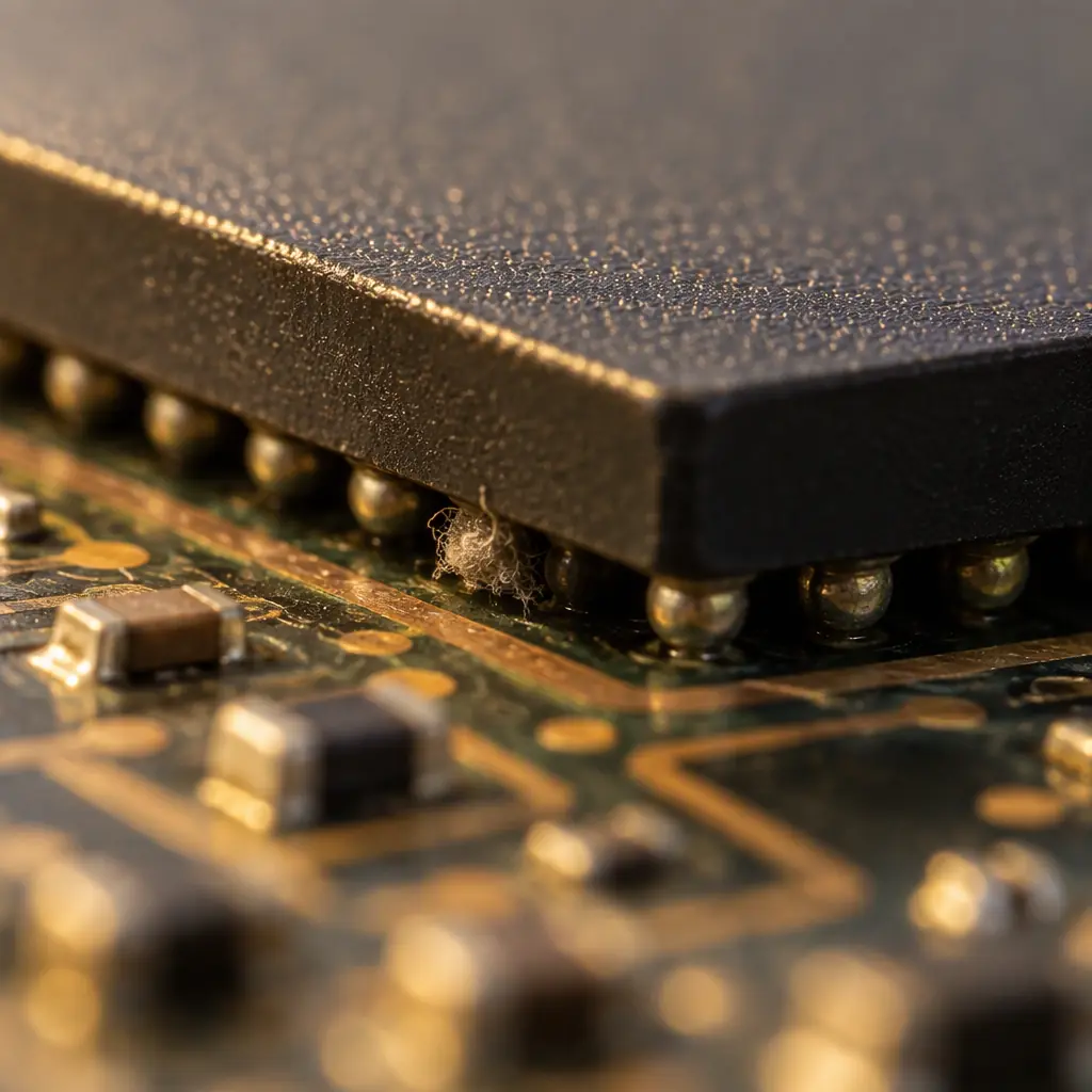
A particle in the gap under a fine-pitch package is invisible to top-down AOI and unreachable by cleaning. This is where latent failures start.
The two most common FOD categories on a PCBA have almost nothing in common, and treating them as one problem is the reason many programmes fix neither.
Solder balls are a process artifact. They form during reflow from paste spatter, from oxygen-driven beading where the flux chemistry and the profile interact badly, or from paste deposits placed where the stencil had a defect. Their distribution is statistical, they cluster around specific component types and specific board regions, and the fix is a process fix: profile, stencil condition, paste chemistry and preheat. The full mechanism and acceptance criteria are set out in solder balling and beading guide. A programme that responds to solder balls by adding inspection is treating a symptom; the defect rate will stay where the process sits.
Loose hardware is a handling artifact. A screw, a wire end, a washer or a piece of tape backing is not generated by the process, it is introduced by a person or a container, and its distribution follows the workstations and the shift patterns rather than the board design. The fix is environmental: tool control, controlled waste containers in the work area, clearance verification at the end of every operation, and a defined point at which the assembly is closed and no further loose articles are permitted. Adding X-ray here does help, but the cheaper intervention is removing the loose articles from the area in the first place.
The practical consequence is that a single FOD control plan with a single owner will usually underperform two plans with two owners and two sets of measures, because the metrics that matter are different. Solder ball rate is measured in defects per million joints and tracked against process parameters. Loose hardware events are measured as line clearance findings per shift and tracked against workstation discipline.
Six Lines That Put FOD Liability on the Supplier
The clause below is written to be inserted into a purchase order or a supplier quality agreement. It does four things: it states the acceptance position, it names the detection gates, it defines what happens on an escape, and it requires notification of a process change that would alter the debris profile.
The supplier shall maintain a documented foreign object debris control programme covering all operations from bare-board receipt to pack-out, including tool control, controlled waste containment within the work area, and a documented line clearance verification at the close of every operation. No loose conductive material shall be present on the assembly at pack-out, and non-conductive material shall be assessed against the electrical clearance requirements of the applicable IPC class. The supplier shall perform automated optical inspection at post-placement on 100% of units and five-axis radiographic inspection on a sample of not less than ten units per lot, and shall make the inspection records available on request. Any unit found to contain loose conductive material after pack-out shall be treated as a nonconformance and supplier's corrective action procedure with a root cause report within ten working days. The supplier shall notify the buyer in writing before implementing any change to stencil supplier, solder paste chemistry, depanel method, or any process that generates particulate debris. Where an escape is attributable to a failure of the programme described in this clause, the supplier shall bear the cost of containment, sorting and return freight.
Each line corresponds to a failure mode that has actually occurred. The line clearance requirement addresses manual assembly debris. The 100% AOI and sampled five-axis line addresses the concealed half of the source table with a measurable number. The ten-unit sample is the minimum that produces a defensible statement about a lot; anything smaller cannot distinguish a clean process from a lucky one. The change notification clause exists because a stencil supplier switch or a change in depanel method can double the debris generation overnight without any process parameter appearing to move. The cost allocation line is the one that makes the rest enforceable.
Eight Questions for a Supplier Audit
The clause is a contract. The audit is how a buyer verifies the programme behind it is real, and eight questions separate a programme from a document.
Ask to see the FOD prevention area map and confirm that the areas marked on it match where your product is actually built. Ask what tool control method is used and to see the shadow board or the tool sign-out log for the line that runs your part. Ask where waste containers sit relative to the assembly stations and whether a container is permitted within the work envelope. Ask what the line clearance procedure is at shift end and at the close of a manual operation, and ask for the last ten completed records rather than the procedure itself. Ask whether AOI runs on 100% of product or on a sample, and what the sample is. Ask whether five-axis or CT capability exists in-house or is subcontracted, and if subcontracted, to whom. Ask how a loose hardware event is recorded and whether the records show any events in the last quarter, since a zero with no records behind it is an absence of measurement rather than an absence of events. Finally, ask what changed in the process in the last twelve months, because a recent change in depanel method or stencil supplier is the highest-probability explanation for a new debris signature.
The answers that should raise a flag are specific. A FOD programme described only in the quality manual with no shop-floor artefact is a document. A tool control system with no sign-out records is an intention. A line clearance record with identical entries across shifts is a form being signed rather than a check being performed. An AOI claim with no sample definition on a concealed-debris product class is a claim about the wrong half of the problem.
Where FOD Fits in the Cost of a Build
The commercial case for a FOD programme is not the rework it prevents, which is small, it is the field return it prevents, which is not. A rework touch on a board costs minutes of labour. A field return caused by a loose conductive particle costs the return freight, the diagnosis, the replacement, the administrative handling, and in regulated product classes the reporting obligation, and it arrives with a failure signature that is difficult to attribute because the debris is often destroyed by the failure it caused.
That asymmetry is why the clause and the audit matter more than the inspection spend. The cheapest FOD control is the one that keeps the material out of the work area, and the second cheapest is the one that catches it before a shield can goes on. Both of those are process decisions made by the supplier, and neither is verifiable from the outside without a clause and an audit. The full inspection framework that surrounds these gates, from AOI through functional test, is set out in PCBA test strategy guide, and the way an escape is traced back to the gate that should have caught it is covered in outgoing quality control page.
FOD on a mainstream commercial PCBA order is usually treated as a housekeeping concern until the first field return, at which point it becomes an expensive one. The programme that prevents it is not complicated: a short source list, a detection gate for each source that names a sample size, a clause that assigns the cost, and an audit that checks the artefacts rather than the manual. The boards that fail in the field are the ones where one of those four was missing.