
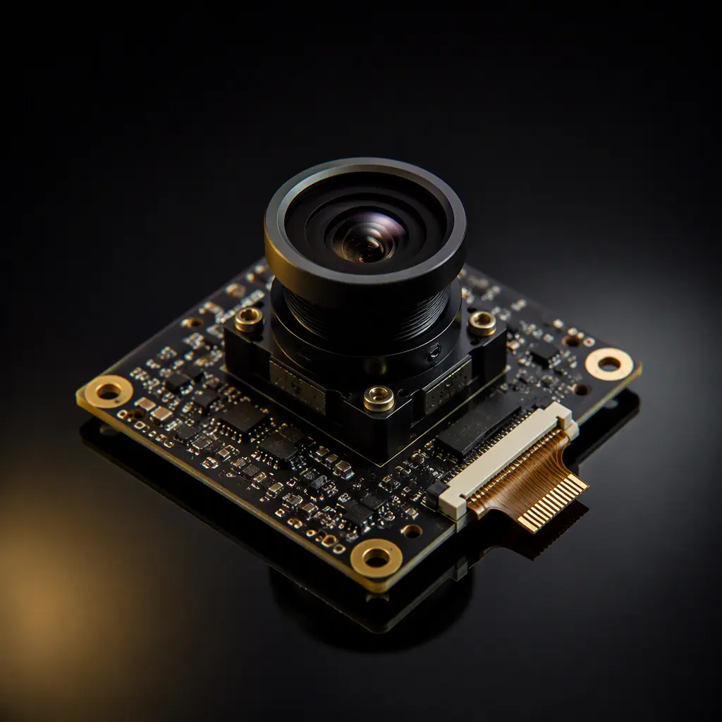
Camera modules are everywhere in 2026 hardware: security cameras, automotive surround-view and cabin cameras, medical endoscopes, machine-vision systems, and AR headsets. A modern image sensor is a precision analog device — a 1/2.3-inch CMOS sensor with 2 µm pixel pitch converts charge to voltage with sub-millivolt accuracy, then pushes that data over MIPI CSI-2 lanes running at 1-2.5 Gbps per lane. The board that carries it must treat the sensor's power and clock with analog discipline while routing high-speed digital lanes that are equally unforgiving.
Huaxing PCBA manufactures camera module boards and host interfaces for security, automotive, and medical customers — 4- to 10-layer controlled-impedance stackups, 100 Ω differential pairs for MIPI lanes, low-noise sensor power regulators, and cleanroom-class assembly for optical components. This guide covers the layout rules that determine image quality, the power and EMI decisions that prevent the classic noise artifacts, and the manufacturing checks to put in your purchase order.
What Lives on a Camera Module Board?
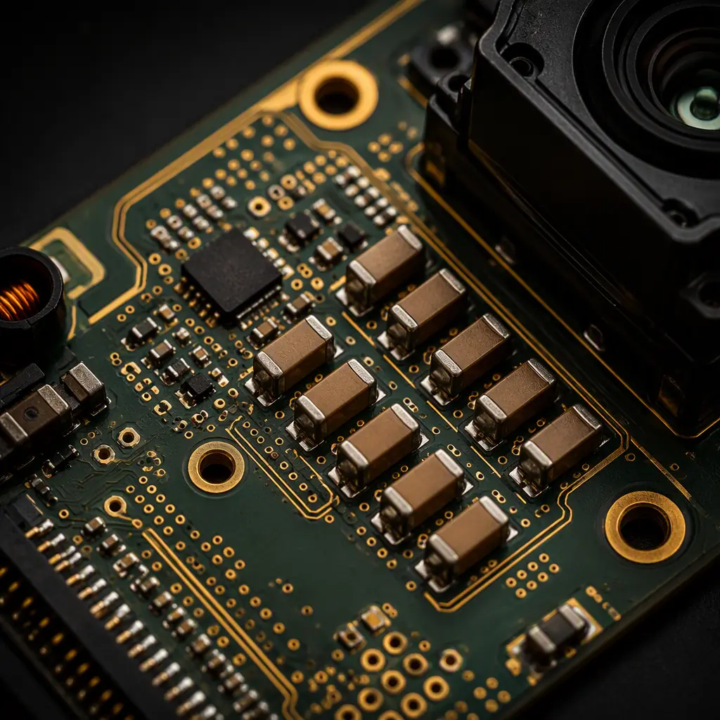
A camera module board is three subsystems on one PCB: the image sensor and its optics, the sensor power and clock tree, and the MIPI CSI-2 output interface. Understanding how these interact is the foundation of every layout decision that follows.
| Subsystem | Typical Components | Key Layout Constraint |
|---|---|---|
| Image sensor | CMOS sensor die, crystal/clock, lens holder, IR filter | Optical alignment, thermal isolation, clean analog supply |
| Power & clock | AVDD/DOVDD/DVDD regulators, MCLK oscillator, decoupling | Noise-free rails — ripple couples straight into pixel data |
| MIPI interface | CSI-2 TX lanes, I2C control, GPIO strobes | 100 Ω differential pairs, length matching, solid reference |
| Interconnect | FPC connector, board-to-board, or flex tail | Impedance through the connector, shielding |
The most common mistake is treating the sensor like a digital chip. It is not — the analog pixel output path sits on the same die as the digital interface, and noise injected into the supply or the substrate shows up as horizontal banding or column noise in the image. Our stackup design guide covers how to allocate layers when a board carries precision analog and high-speed digital together.
MIPI CSI-2 Routing: The Rules That Prevent Dropped Frames
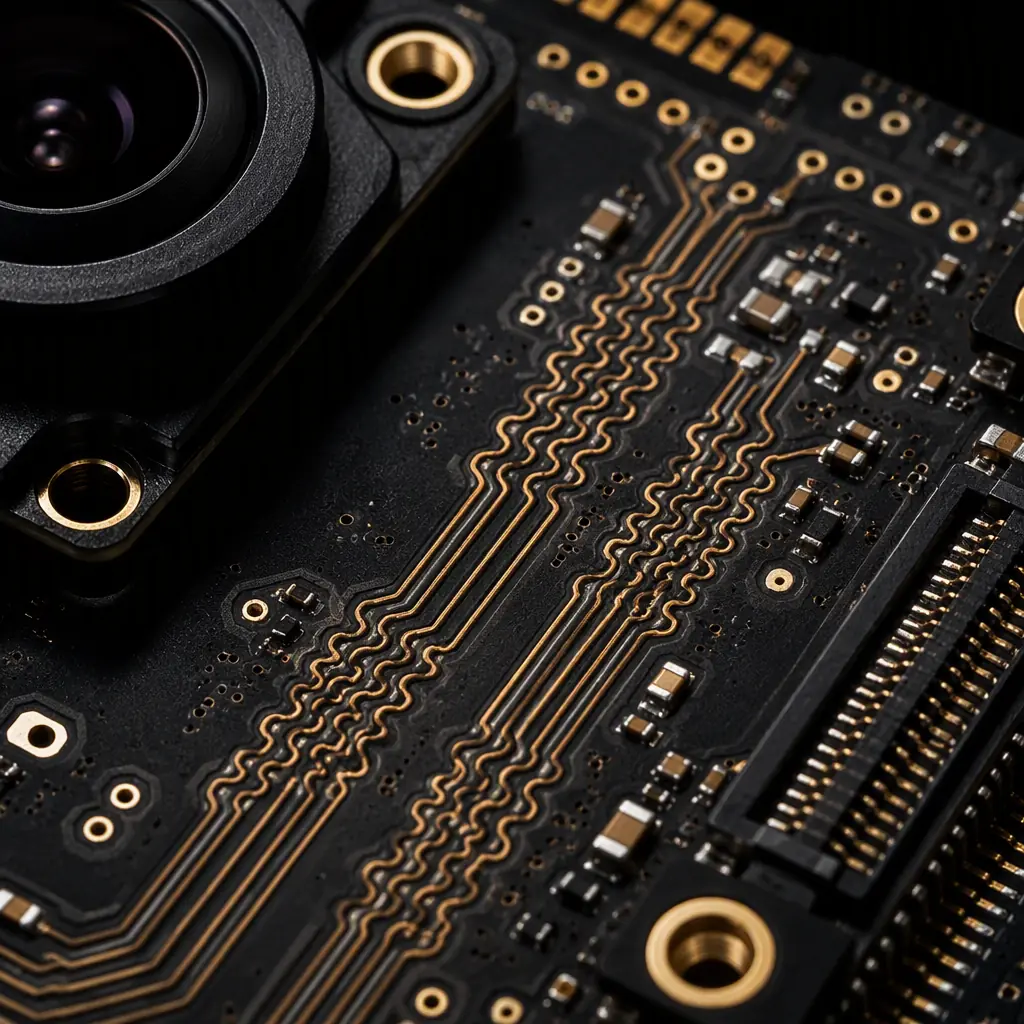
MIPI CSI-2 carries the image data from sensor to processor as differential pairs — one clock lane and one to four data lanes, each pair running at 1-2.5 Gbps depending on resolution and frame rate. A 4K@60 sensor with 4 lanes pushes roughly 2.5 Gbps per lane, which puts the layout squarely in high-speed signal-integrity territory.
Route MIPI Lanes as 100 Ω Differential Pairs With Controlled Impedance
Each MIPI pair must be routed as a differential pair with 100 Ω differential impedance (85 Ω on some automotive applications), with a continuous ground reference directly beneath. Specify the impedance target on the fabrication drawing — it is not negotiable at these data rates. Keep the pairs away from the sensor's analog supply traces and from the MCLK clock line. Our signal integrity guide has the pair-routing rules, and the impedance control guide covers how to specify targets.
Match Lane Lengths Within 5-10 mil
All data lanes and the clock lane must be length-matched so the pixel data arrives at the processor in the same cycle. Typical tolerance is 5-10 mil (0.13-0.25 mm) between lanes and slightly looser between data and clock. Length matching is done with serpentine routing in the pair itself — never route one lane of a pair on a different layer, because the via delay alone can exceed the tolerance. Our backdrilling guide covers via effects on high-speed lanes.
Minimize Vias on MIPI Lanes — and Ground Them When You Can't
Each via on a MIPI lane adds 5-10 ps of delay and an impedance discontinuity. Keep the lane count low (2-4 vias per pair maximum) and place ground vias beside signal vias to preserve the return path. If the sensor and processor are on different boards connected by an FPC, the FPC's impedance and the connector's transition become part of the link — specify the FPC impedance and keep the tail short. Our flex PCB guide covers FPC impedance and bend requirements.
Key Takeaway: MIPI failures rarely show up as "no image" — they show up as intermittent frame drops, sparkle on the display, or heat-related glitches that pass QC in the lab and fail in the field. The layout rules above exist precisely because these intermittent faults are nearly impossible to catch in production testing. Get the routing right before tooling.
Sensor Power: The Analog Discipline That Kills Banding
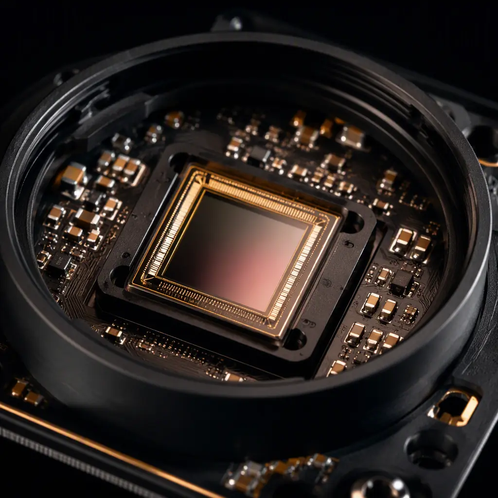
An image sensor needs three or more supply rails — AVDD (analog, typically 2.8 V), DOVDD (digital I/O, 1.8 V), and DVDD (digital core, 1.1-1.2 V) — and the separation between them is a layout decision, not a schematic one. Noise on AVDD appears in the image as horizontal banding or fixed-pattern noise, and it is the #1 image-quality defect we see in camera boards.
Keep the Analog Supply Separate From the Digital Supply
AVDD must be generated by its own LDO (or a dedicated regulator output) with the ferrite bead and decoupling network from the sensor datasheet — never shared directly with the digital rail. Route the AVDD trace as a short, wide trace or a local plane segment that does not cross digital switching traces. A 10-20 mV ripple on AVDD is enough to create visible banding on a 12-bit sensor. Our power integrity guide covers rail isolation and decoupling in depth.
Follow the Power-Up Sequencing Requirements
Most sensors require AVDD before DOVDD before DVDD (or a specific sequence from the datasheet), with the reset pin held until all rails are stable. This is normally handled by a PMIC or supervisor IC, but the layout must keep the enable/reset traces short and free of noise so the sequence is reliable. A sequencing violation can latch the sensor into a low-quality mode that passes basic image tests and fails at low light.
Place Decoupling Within 2-3 mm of Every Sensor Power Pin
The sensor's decoupling capacitors — typically 0.1 µF and 1 µF or 4.7 µF per rail — must sit within 2-3 mm of the corresponding pin, on the same layer or through a single via pair. Long decoupling traces add inductance that defeats the capacitor's purpose at the frequencies the sensor switches. Our mixed-signal design guide explains the ground and decoupling strategy for analog-digital coexistence.
Clock, EMI, and the MCLK Discipline
The sensor master clock (MCLK, typically 24-27 MHz) drives the entire pixel pipeline, and its harmonics are a classic radiated-emissions problem. A 27 MHz fundamental with sharp edges generates harmonics that land directly in FM radio and other bands, and the clock line couples into the MIPI lanes if routed carelessly.
Route MCLK as a Guarded Trace, Not a Bus Signal
The MCLK trace should be short, routed over a solid ground, with ground guard traces or ground vias alongside if it runs more than 10-15 mm. Do not route it parallel to MIPI lanes or to the I2C control lines. Series termination (typically 22-33 Ω) at the driver matches the impedance and rounds the edges, cutting harmonic energy. Our EMC compliance guide covers clock-line emission control in detail.
Plan the EMI Budget at Kickoff, Not at the Lab
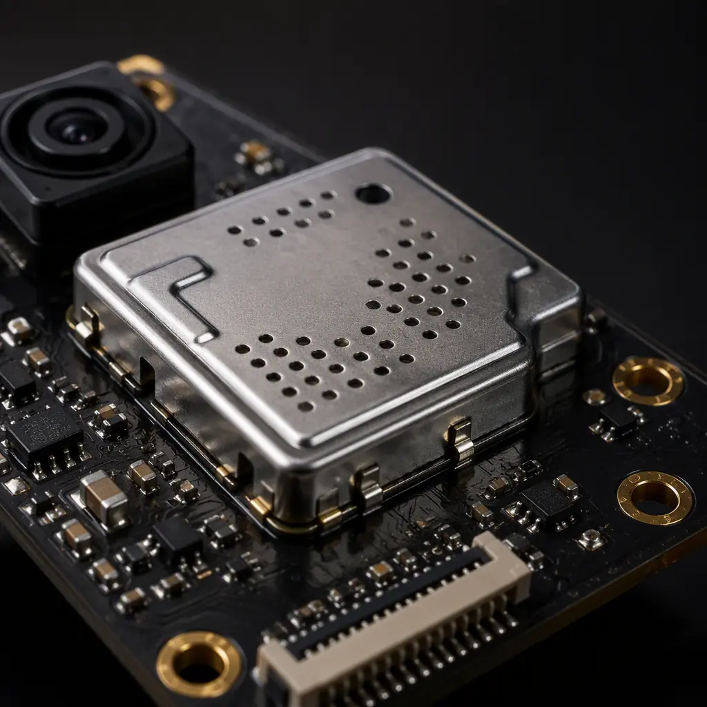
Camera boards fail FCC/CE radiated testing more often than most products because the sensor clock, the MIPI lanes, and the FPC connector radiate as a system. Decide the target (FCC Part 15B, CE, or automotive CISPR 25) at project start, and carry the margin into the layout: shield cans over the sensor and the clock source, a grounded FPC connector shell, and a continuous ground plane under the whole camera area. Our EMI/EMC design guide has the full emissions-control checklist.
Consider Spread-Spectrum Clocking for Consumer Products
Many sensor platforms support spread-spectrum clocking (SSC) on MCLK, which spreads the clock energy across a small frequency range and reduces peak emissions by 3-6 dB. SSC is a firmware/configuration choice, but the layout must accommodate it — the decoupling and termination rules are the same. For security and automotive cameras where certification is strict, the combination of SSC and a shield can is the standard recipe. Our security camera PCB guide covers the system-level EMC approach.
Optical and Thermal: The Mechanical Side of Image Quality
Image quality is not only electrical. The sensor's performance degrades with temperature — dark current doubles roughly every 6-7 °C — and the optical path (lens, IR filter, focus) is a mechanical assembly that the PCB must support precisely.
Keep the Sensor Thermally Connected to a Heat Path
The sensor package should have a thermal pad connected through thermal vias to a ground or dedicated thermal plane. At 60 °C junction, a typical sensor's dark current and hot-pixel count rise noticeably; at 80 °C, image quality in low light degrades visibly. For outdoor security cameras, specify the thermal budget (ambient + self-heating) and verify with a thermal simulation or prototype measurement. Our thermal management guide covers via arrays and heat spreading.
Design the Footprint for Optical Alignment
The sensor's optical center must align with the lens holder and the enclosure aperture. Use fiducials on the board and specify the sensor placement tolerance (±0.05 mm or better) in the assembly drawing. For automotive and medical cameras, active alignment (adjusting the lens while the sensor is live) is common — the PCB must allow access for the alignment fixture and the adhesive cure. Our DFT guide covers fiducial and test-point design.
Cleanroom-Level Assembly for the Optical Path
Dust on the sensor window or the IR filter is a permanent image defect. Camera module assembly should happen in a cleanroom or at minimum a controlled environment with ESD protection, with the sensor kept in its sealed packaging until the last step. If your manufacturer does not offer clean assembly for optical components, image defects will appear in the field and be blamed on the sensor. Our ESD control guide covers the handling requirements.
Manufacturing Checks for Camera Boards
Camera module boards combine the tightest tolerances of any consumer PCB: controlled impedance, fine-pitch sensor packages (often 0.4-0.5 mm pitch BGA or LGA), optical alignment, and cleanliness. The manufacturing partner you choose must be qualified for all of it.
Impedance Control With Coupons on Every Panel
The 100 Ω differential pairs on MIPI lanes need impedance coupons on every panel with measured values reported. Verify the target is on the fab drawing — a drawing that omits impedance targets while the layout assumed 100 Ω pairs is the most common camera-board DFM failure. Our tolerances guide covers impedance verification in production.
X-Ray Inspection for Fine-Pitch Sensor Attach
Image sensors in LGA or BGA packages need X-ray inspection of the solder joints — hidden voids under the die can cause intermittent failures that appear as image glitches months later. Require 100% X-ray for the sensor attach, or at minimum on the first article and lot samples. Our AOI vs X-ray guide explains when each method is mandatory.
Functional Image Testing Before Shipment
Every camera module should be powered up and capture a test image before shipment — a flat-field check catches dead pixels, banding, and focus defects that electrical test cannot. For security cameras, a test chart shot verifies the whole optical path. Specify "100% functional image test with flat-field and test-chart capture" in your purchase order; manufacturers who cannot do this are not equipped for camera work.
Summary: The Camera Board Checklist
A camera module board that delivers clean images routes MIPI lanes as controlled 100 Ω differential pairs with matched lengths and minimal vias, isolates the analog sensor supply from digital noise, disciplines the MCLK with termination and guards, plans the EMI budget before the first prototype, keeps the sensor cool and clean, and verifies every board with X-ray and functional image testing.
At Huaxing PCBA we manufacture camera module boards with controlled-impedance stackups to 10 layers, 100 Ω MIPI differential pairs, low-noise sensor power stages, cleanroom-class assembly for optical components, X-ray inspection of sensor attach, and 100% functional image testing before shipment. Our DFM review checks the MIPI lane routing, length matching, sensor decoupling, thermal via array, and test access before tooling. Read our security camera PCB guide to prepare your design, or send your files for a free DFM review and quote.
