
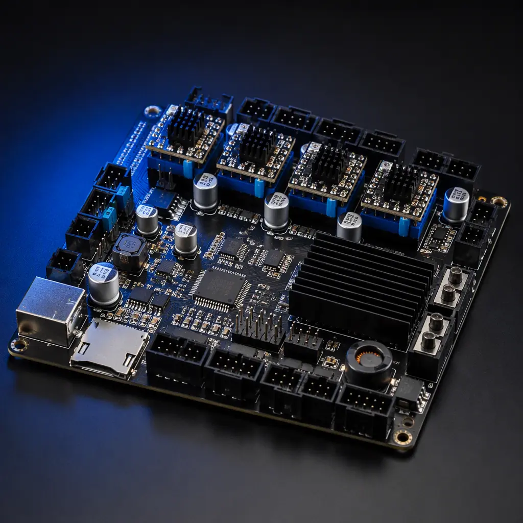
A modern FDM 3D printer mainboard is a power electronics board wearing a motion-control hat: four to six stepper drivers switching 1–2 A per phase, a heated bed pulling 200–350 W, a hotend heater, a part-cooling fan, and a 32-bit MCU coordinating all of it — usually on a single 4-layer PCB. Get the power stage right and the printer prints quietly for years; get it wrong and you get thermal runaway shutdowns, ghosting in the prints, and EMC failures at certification.
Huaxing PCBA manufactures 3D printer mainboards and heated-bed PCBs for printer OEMs and aftermarket brands — up to 6 layers, 2 oz and 3 oz copper for heater and motor paths, 24 V architectures to 350 W, and 100% functional test with heater and stepper loads connected. This guide covers the component and layout decisions that separate a 2026-quality mainboard from a hobby-grade one.
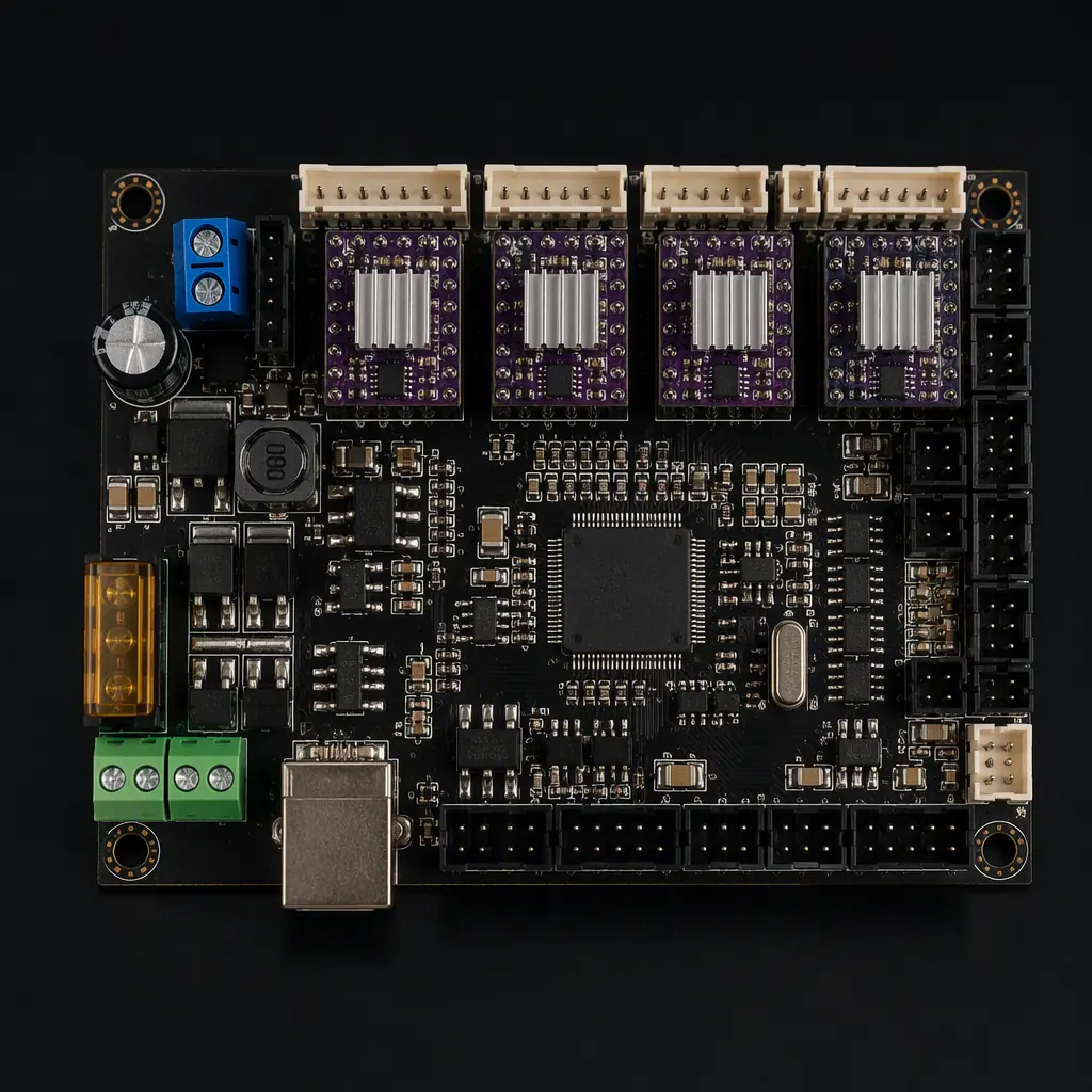
Anatomy of a 3D Printer Mainboard: What Actually Lives on the Board
The board is a small power plant with a motion controller attached. Every subsystem has a PCB consequence:
| Subsystem | Typical Spec (2026) | PCB Consequence |
|---|---|---|
| MCU | 32-bit (STM32, RP2040, ESP32 class) | 3.3 V logic, quiet digital ground |
| Stepper drivers | 4–6× TMC2209/TMC5160 class, 1–2 A RMS | Solid thermal pad, sense resistors, quiet SPI/UART lines |
| Heated bed | 24 V, 200–350 W (9–15 A) | 2–3 oz copper, MOSFET with heatsink, thick traces |
| Hotend heater | 24 V, 40–70 W | MOSFET switching, thermistor input accuracy |
| Power input | 24 V DC, 300–500 W PSU | Reverse-polarity protection, bulk capacitance, inrush control |
| Connectivity | USB, Wi-Fi, SD card, display port | ESD protection on every external connector |
The layer count is almost always 4: two signal layers plus a solid ground plane and a power plane. The ground plane is what makes the difference between a board that prints cleanly and one with layer-shift artifacts from motor noise coupling into the endstop and encoder inputs. Our layer count selection guide explains the 2 vs 4 layer decision for mixed power/digital boards.
Stepper Motor Drive: Current, Microstepping, and Quiet Operation
The stepper drivers are the heart of print quality. Their selection and layout determine the two things buyers actually notice: print accuracy and noise.
| Driver Class | Typical Current | Microstepping | Noise Behavior | Typical Use |
|---|---|---|---|---|
| A4988 class (legacy) | 1–2 A | Up to 1/16 | Audible whine at low speeds | Budget printers, retired |
| TMC2209 class | 1.4–2 A RMS | Up to 1/256 | StealthChop — near-silent | Mainstream 2026 printers |
| TMC5160 class | 2–3 A RMS | Up to 1/256 | Silent with spreadCycle control | CoreXY, large-format, high-speed |
Design the Driver Thermal Path for Continuous Current
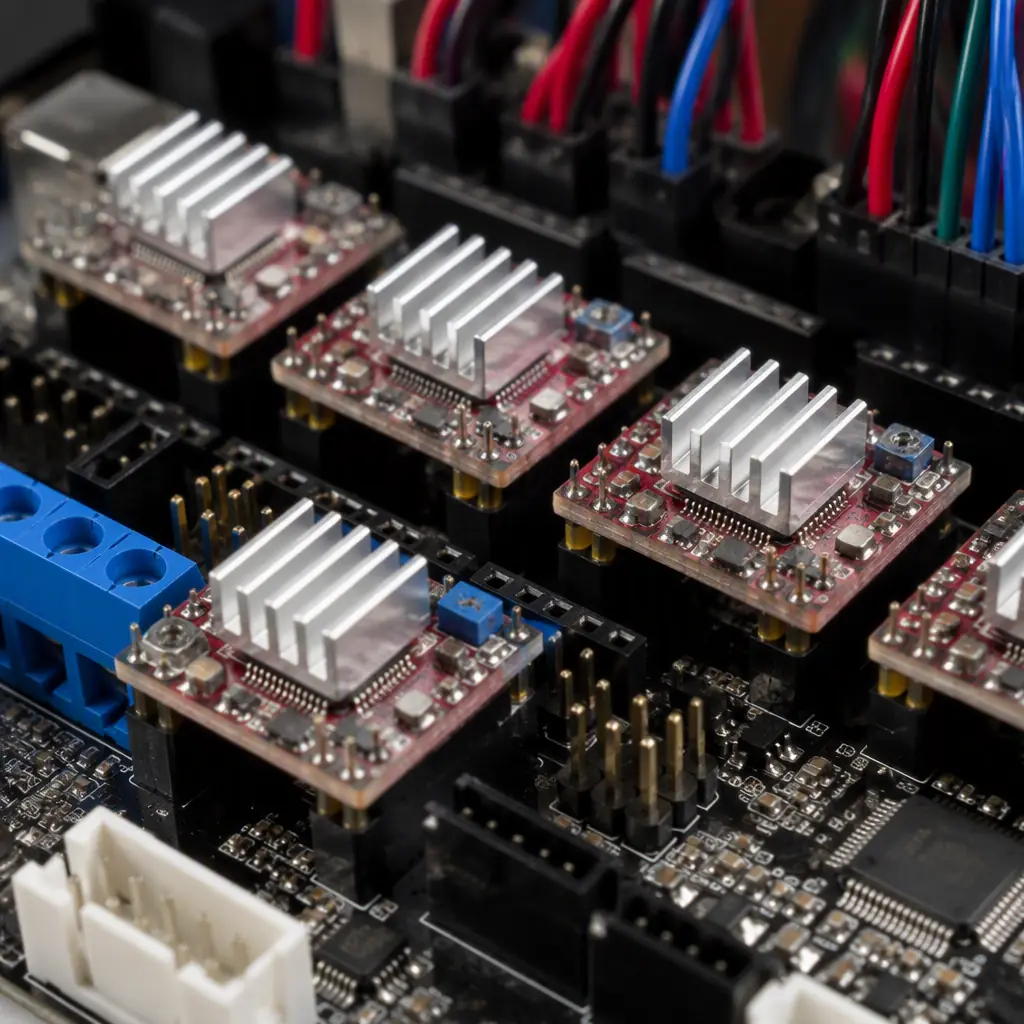
Stepper drivers run at 1–2 A RMS continuously, hour after hour. The exposed pad must be soldered to a copper island with thermal vias to the ground plane — a driver without a thermal path derates itself and can hit thermal shutdown mid-print. Require X-ray or AOI verification of the driver pad solder coverage in assembly. Our thermal management guide covers pad and via design for power components.
Keep the Current-Sense Path Short and Clean
The driver's current regulation measures voltage across a sense resistor on the motor return path. Any parasitic inductance or resistance in that path shifts the actual motor current. Put the sense resistors within a few millimeters of the driver, use 1% low-inductance parts, and route the sense traces as a tight differential pair to the driver pins. Our power integrity guide has the sense-resistor layout rules.
Run the Driver Interface as a Quiet Bus
Modern drivers communicate over UART or SPI for current and microstepping configuration. These lines run next to switching motor phases on the same board — route them on the inner signal layer between ground planes, and add series resistors (22–33 Ω) at the driver pins to damp ringing. A corrupted UART configuration mid-print is the kind of intermittent failure that takes weeks to find.
Heater Control: Sizing the Heated-Bed MOSFET for 350 W
The heated bed is the highest-current subsystem on the board, and the most common source of field failures — usually because the MOSFET was sized for the bed's steady-state power instead of its switching reality.
Do the 24 V Math Before Picking the MOSFET
A 300 W bed at 24 V draws 12.5 A. A logic-level MOSFET with 5 mΩ RDS(on) dissipates about 0.8 W of conduction loss at that current — fine thermally with a pad. But the switching loss at 1–10 kHz PWM, plus the cold-bed inrush (a cold bed's resistance is roughly 30% lower, so it draws more current at power-on than at operating temperature), means the part must be rated for the peak, not the average. Select a MOSFET with at least 2× the calculated current headroom and verify the thermal pad area in the layout. Our trace width and current capacity guide has the copper sizing tables for the 12.5 A path.
Route the Bed Power Path as a Low-Inductance Loop
The loop from the input connector through the MOSFET and back to the bed connector should be short and wide — the switching node is where the EMI radiates from. Keep the MOSFET gate drive close to the MOSFET, add a gate resistor (10–22 Ω) to control slew rate, and put a snubber across the switching node if the layout forces a long run to the bed connector. Our SMPS layout guide covers switching-node discipline in depth.
Independent Thermal Fuse Path — Never Rely on Firmware Alone
A runaway heated bed is a fire hazard, and firmware thermal runaway detection has failure modes (frozen MCU, corrupted sensor reading). The board should include a hardware thermal cutoff — a thermal fuse or a dedicated hardware comparator on the bed thermistor that latches the MOSFET off — independent of the MCU. Print this requirement in the spec; it is a liability line, not a feature. Our functional safety guide covers the independent-fail-safe principle in the automotive context that applies here too.
Thermal Sensing: Thermistor Accuracy That Doesn't Drift
Print temperature accuracy is set by the thermistor circuit, and most temperature complaints trace back to the PCB, not the sensor.
Use 100 kΩ NTC (B = 3950) With a Precision Reference
The de-facto standard is a 100 kΩ NTC thermistor with B = 3950, read through a voltage divider with a 4.7 kΩ pullup to a stable reference. At 200–300 °C the divider output sits in the middle of the ADC range where accuracy is best. Use a 0.1% pullup resistor and a dedicated reference if the MCU's VDD tolerance is loose — a 3% reference shift reads as 5–10 °C of error at hotend temperatures.
Keep the Thermistor Traces Away From the Heater Lines
The thermistor signal is a high-impedance divider output — a few hundred mV of coupled noise from the adjacent heater MOSFET switching changes the temperature reading and can trigger false thermal-runaway shutdowns. Route thermistor traces on the inner layers between ground planes, or shield them with a ground trace on both sides. Our MCU PCB design guide covers ADC input conditioning and grounding.
Calibrate the Beta Curve in Production, Not in the Field
Thermistor B-value tolerance (±1% on good parts) plus ADC error adds up to a per-unit temperature offset. For brands that advertise ±1 °C hotend accuracy, the manufacturing line should calibrate each board's temperature mapping during functional test — a 30-second step that eliminates most "temperature too high/low" support tickets. Our first-article inspection guide shows how to build calibration into the test fixture.
Power Input: 12 V vs 24 V Architectures and Inrush
The 2026 mainstream is 24 V, and the migration changed the PCB rules substantially.
24 V Halves the Current, But Doubles the Layout Discipline
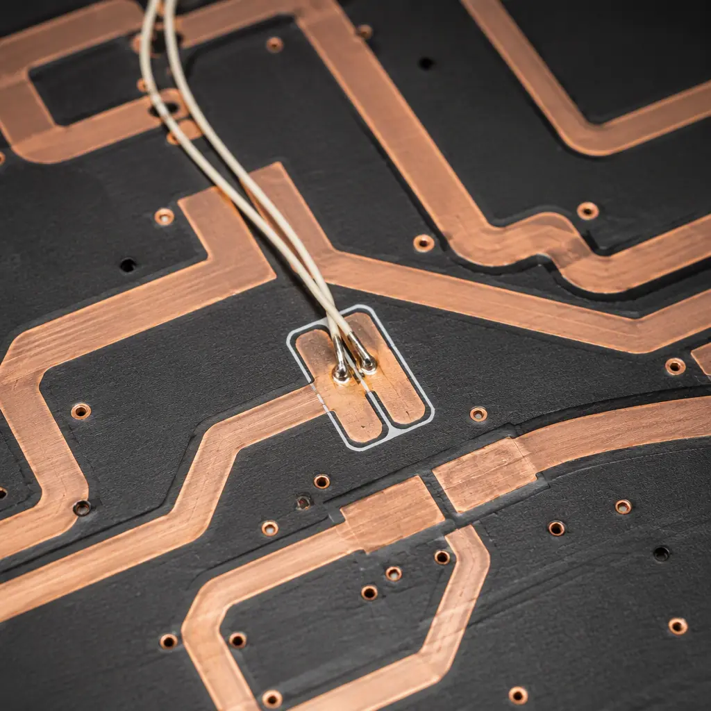
Moving from 12 V to 24 V cut the bed current from 25 A to 12.5 A for the same wattage — smaller traces, smaller MOSFETs, less heat. The trade-off: higher voltage stresses on the switching nodes and connectors, and a bigger safety gap requirement between high-voltage traces. Specify creepage/clearance per the working voltage (IPC-2221B) and review the connector ratings — a cheap 24 V connector is a field-failure generator. Our high-voltage design guide covers the spacing rules.
Handle the Cold-Bed Inrush at Power-On
A cold bed's resistance is roughly 30% lower than at operating temperature, so at power-on the bed draws ~1.3× its steady-state current — plus the PSU's own inrush and the bulk capacitors charging. Without soft-start, the connector and PSU see a current spike that degrades contacts over time. An NTC inrush limiter on the input or firmware-controlled PWM ramp (500 ms) solves it cheaply. Our SMPS layout guide covers bulk capacitance and inrush handling in detail.
Reverse-Polarity and ESD Protection on Every Input
The barrel jack or XT60 input is user-pluggable — a reversed connector is a common user error that should cost a fuse, not a mainboard. Include reverse-polarity protection (P-channel MOSFET ideal-diode circuit or a beefy Schottky), a slow-blow input fuse sized at 1.5× max current, and TVS clamping on the input. Our ESD control guide covers connector protection practice.
EMI From Steppers: Why Print Quality Degrades and How to Fix It
A printer with five switching motor phases, a PWM bed heater, and a fan controller is an EMI source by construction. The failures show up two ways: radiated emissions failing FCC/CE at the lab, and internal coupling that corrupts the MCU, the endstops, or the Wi-Fi module during prints.
Design for the Motor Cable, Because the Cable Radiates
Motor cables are the antennas. Plan for ferrite beads on each motor cable near the connector, twisted-pair wiring in the harness spec, and keep the connectors grouped at one board edge so cables don't crisscross the enclosure. The board layout can't fix a bad cable harness — but it can make the cable the only radiating element, which is manageable. Our EMI/EMC design guide has the full emissions checklist.
Keep Switching Nodes Off the Outer Layers
The bed-heater and stepper switching nodes should live on inner layers or be shielded by ground pour on both sides. A switching node on the outer layer next to the board edge radiates directly. If the layout forces an outer-layer switching trace, run a ground trace beside it and keep it short. Our signal integrity guide covers return-path and shielding discipline.
Test With All Motors Moving and the Bed PWMing
An EMC pre-scan with the printer idle passes; with all five steppers stepping and the bed at full PWM, it can fail by double digits. Put "EMC pre-compliance with full motion profile" in the development plan and run it before the certification submission. Our EMC compliance guide explains how to specify pre-scan testing to your manufacturer.
Assembly and Testing for Mainboard Reliability
3D printer mainboards run hot, vibrate, and get handled by enthusiasts who probe around with multimeters. The manufacturing checks should match that life.
Functional Test With Real Loads, Not Just Connectivity
Require a functional test that connects actual steppers and heaters: verify each driver steps, each heater reaches target temperature, the thermistor reads within calibration, and the fans spin. A connectivity-only ICT misses a weak driver thermal joint that only fails under load. Our test method guide explains the three test tiers.
AOI Plus X-Ray on the Driver and MOSFET Pads
Stepper drivers and power MOSFETs fail silently when their thermal pads have voids. AOI catches the visible defects; X-ray catches the voids under the exposed pads. Specify X-ray sampling (e.g., 5 boards per lot) on the power components, with void acceptance per IPC-A-610. Our AOI/X-ray/SPI guide has the acceptance criteria.
Burn-In the Power Stage Before Shipping
A 30–60 minute powered burn-in with the bed at temperature catches the early-life failures — marginal MOSFETs, cold solder joints under thermal stress, weak connectors — before they reach customers. For higher-volume SKUs, sample-based thermal cycling adds another layer of confidence. Our burn-in and ESS guide has the profiles.
Summary: The 3D Printer Mainboard Checklist
A 2026-quality 3D printer mainboard is a 24 V power board with disciplined motion control: drivers with real thermal paths and quiet interfaces, MOSFETs sized for cold-bed inrush, thermistor circuits that don't drift, a hardware thermal fail-safe, and EMI managed at the layout stage with the motor cables in mind. The manufacturers who ship quiet, reliable printers treat these as PCB rules — not firmware features.
At Huaxing PCBA we manufacture 3D printer mainboards and heated-bed PCBs up to 6 layers with 2–3 oz copper, 24 V architectures to 350 W, and functional test with real stepper and heater loads. Our DFM review checks driver thermal pads, heater-loop inductance, thermistor trace isolation, and connector ratings before tooling. Read our MCU board design guide to prepare your design, or send your files for a free DFM review and quote.
