
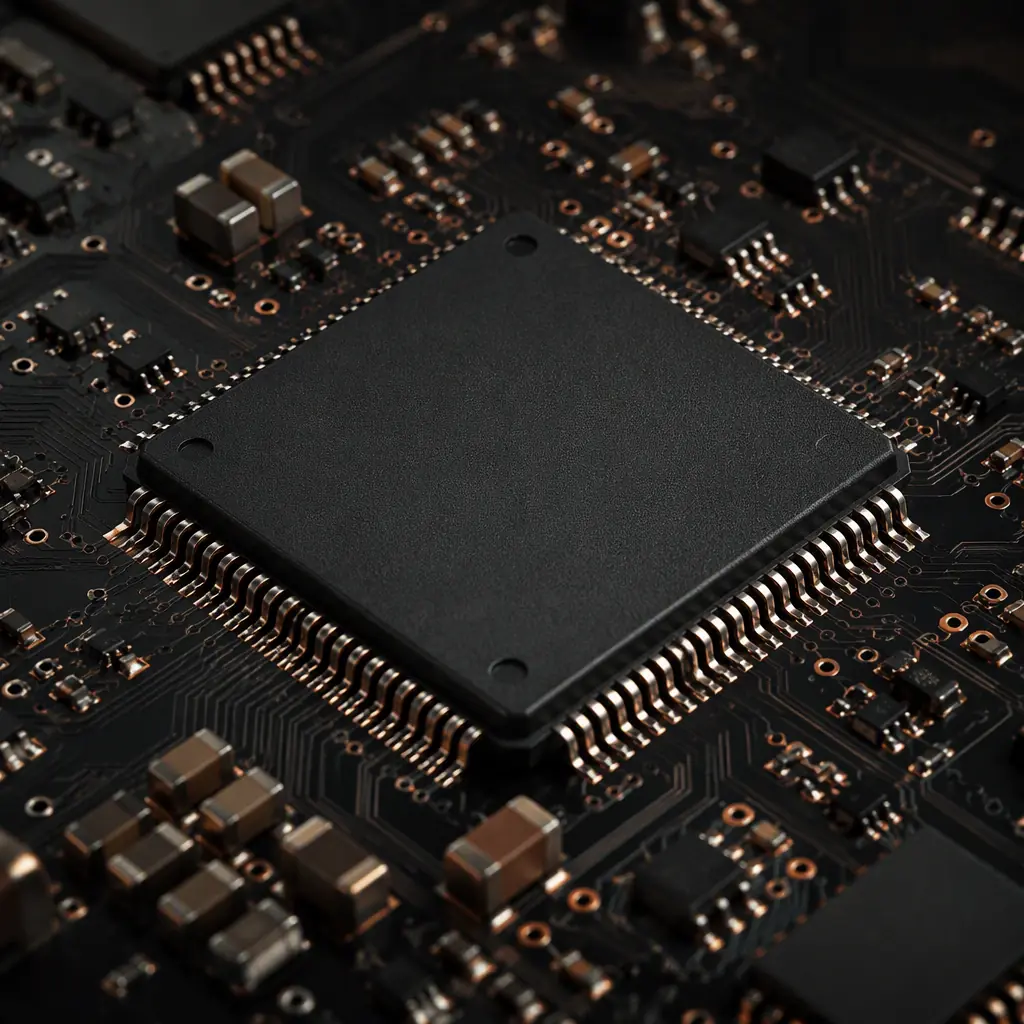
Microcontrollers are forgiving — until they are not. The same MCU that runs happily on a poorly laid-out prototype board will glitch in production: brown-out resets on motor start, ADC readings that wander with the display update, a crystal that fails to start at cold temperature, or SWD programming that only works with a specific cable length. These are the classic symptoms of layout problems, and they are entirely preventable with a few disciplined rules applied at the schematic and layout stage.
Huaxing PCBA manufactures and assembles embedded control boards — from 2-layer sensor nodes to 32-layer industrial controllers — across 8 SMT lines with 0201 placement and 0.3 mm-pitch QFN/BGA capability, under ISO 9001 and IATF 16949. This guide covers the MCU-specific layout rules that matter most, plus the DFM details that determine whether your QFN or QFP board assembles cleanly the first time.
Layer Stackup — When Is 2 Layers Enough, When Do You Need 4
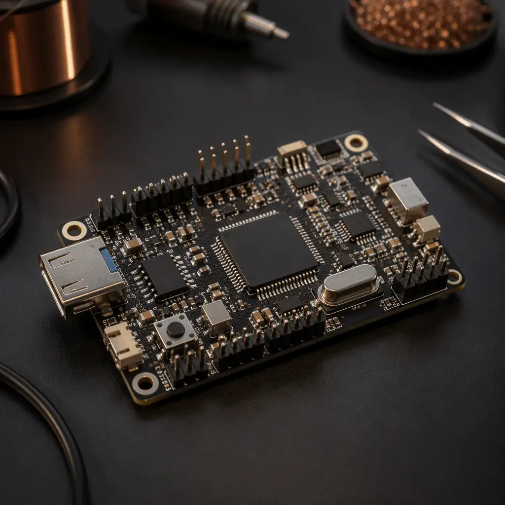
The stackup decision sets the ceiling for everything else. For a simple MCU board with a few GPIOs, one UART, and no analog precision requirement, a 2-layer board is fine. For anything with an ADC you care about, a switching regulator, or high-speed communication, a 4-layer board is cheaper than the field failures it prevents.
| Board type | 2-layer | 4-layer |
|---|---|---|
| Stackup | Signal / Signal | Signal – GND – PWR – Signal |
| Ground reference | Partial pours, weak | Solid plane, continuous |
| ADC accuracy | ±10–20 LSB noise floor typical | ±1–3 LSB achievable with care |
| Decoupling effectiveness | Loop inductance limited | Cap-to-plane inductance minimal |
| EMI behavior | Higher emissions | Controlled return paths |
| Typical cost delta | — | +30–60% board cost |
The rule of thumb: if the product has a precision ADC, a radio, or a motor/relay switching on the same board, go 4-layer. The ground plane directly under the MCU gives every decoupling capacitor a low-inductance return path, which is the single biggest lever on MCU stability. Our stackup design guide walks through the layer-count decision in detail.
Key Takeaway: Four layers for anything with analog precision or noise sources; two layers only for simple digital-only boards. The ground plane is the foundation of every other rule in this guide.
Power Delivery and Decoupling — Placement Is Everything
MCU datasheets specify decoupling values — typically 100 nF per power pin plus one 1–10 µF bulk cap per supply domain. The values matter less than the placement. A 100 nF cap 10 mm from the pin has so much loop inductance that it is nearly useless at the frequencies the MCU switches at (tens to hundreds of MHz).
Place the 100 nF Caps Within 2 mm of Their Power Pin
Each VDD/VCC pin gets its own 100 nF cap, placed on the same side of the board as the MCU, as close to the pin as the footprint allows — the via-to-pad distance plus the cap body should fit within roughly 2 mm. Route power from the pin to the cap first, then to the via; keep the ground side short to the via. This creates the smallest possible charge loop. If the MCU has a central power pad (QFN), the vias go under the body — see the DFM section below.
One Bulk Cap Per Supply Domain, Close to the Source
Place a 4.7–22 µF bulk capacitor near where the supply enters the MCU area — at the output of the regulator or where the connector power comes in. It handles the low-frequency transients (motor starts, radio bursts, display refresh) that the 100 nF caps cannot. For mixed analog/digital supplies, isolate the analog rail with a ferrite bead or a small series inductor and its own bulk cap — see our power integrity guide for the full PDN design process.
Keep the Regulator Loop Tight and Away From Analog
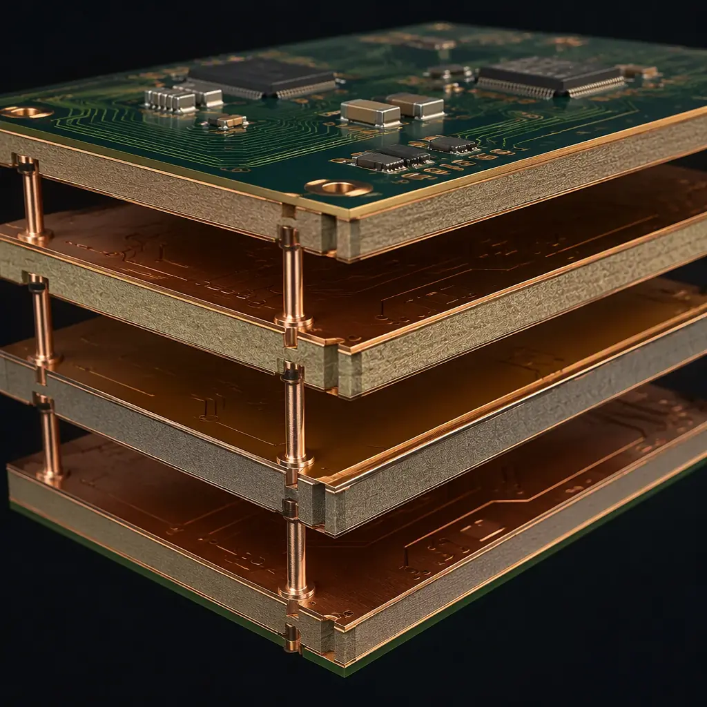
If the board has a buck converter, keep its switching loop (input cap, inductor, output cap) compact, and route the switch node (LX) as a short wide trace on one layer with the ground return directly beneath. Do not route the switch node under the MCU, the crystal, or the ADC section. A ferrite bead between the digital 3.3 V and the analog supply (AVDD) is the standard isolation method for MCU ADC accuracy.
Crystal and Oscillator Layout
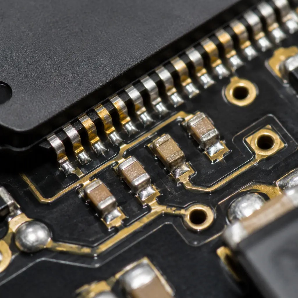
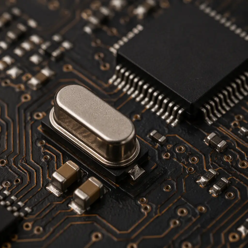
Crystal circuits are sensitive by nature: a few picofarads of stray capacitance, a noisy trace underneath, or a ground cut under the crystal can prevent startup or cause frequency drift. The MCU's internal oscillator amplifier is also a broadband noise source that can couple into adjacent analog circuits.
Keep the Crystal Close to the MCU Pins — No Vias in the Loop
Place the crystal within 5–10 mm of the MCU's OSC pins. Route the two crystal traces short, symmetric, and on the same layer, with no vias in the loop. Do not route any other signal underneath the crystal area on adjacent layers — add a ground pour (or a guard ring) around and under the crystal footprint and stitch it with vias. A via under a crystal pad is a classic intermittent-startup source.
Size the Load Capacitors Correctly — and Check the MCU's Internal Capacitance
For a parallel-resonant crystal, the load capacitance CL is specified on the crystal datasheet. The two external load caps are typically 2 × CL (minus the MCU pin and PCB stray capacitance, roughly 3–5 pF). For an 8–16 MHz crystal with CL = 18 pF, two 22 pF caps are the common starting point; for CL = 12 pF, two 15 pF caps. Many modern MCUs have internally adjustable load capacitance — check the reference manual and disable internal caps if you are using external ones. A series resistor of 0–33Ω in the OSC_OUT path limits drive level and prevents crystal overdrive.
32.768 kHz RTC Crystals Get the Same Discipline
The low-frequency RTC crystal is even more sensitive — it runs at microwatt drive levels. Keep its traces short, guard them with ground, and keep the RTC crystal and its caps away from any switching node or the MCU's main crystal. If the RTC must stay accurate, the load capacitance (typically 6–12.5 pF for watch crystals) must match the crystal spec exactly; mismatch shifts the frequency by tens of ppm.
Analog Grounding for ADC Accuracy
The classic MCU ADC symptom: readings jump when the display updates or when a relay switches. The cause is usually a shared ground return or a noisy reference. The fix is partitioning — not splitting planes arbitrarily.
Partition the Board Into Digital and Analog Zones
Group all analog circuitry (ADC inputs, reference, sensor front-end, op-amps) into one zone, and keep digital switching (MCU, communication interfaces, regulators) out of it. On a 4-layer board with a solid ground plane, the standard approach is a single ground plane with a moat or slot under the analog zone, connected to the digital ground at one point — ideally under the MCU, where the ADC reference and ground pins are. Our mixed-signal design guide covers star grounding and partitioning in detail.
Give the ADC a Clean Reference
If the MCU has a separate VREF pin, route it as a quiet trace directly from the reference source (a dedicated reference IC, or the analog supply through an RC filter) — never from the digital 3.3 V rail without filtering. Keep the reference trace away from the crystal and the switch node. For 12-bit and higher ADCs, use a 0.1 µF + 1 µF cap directly at the VREF pin with a tight ground return.
Filter and Guard Analog Input Traces
Route ADC input traces away from digital lines, add a small RC filter (e.g., 1 kΩ + 1 nF) at each analog input if the source impedance and sample rate allow, and keep the analog source ground return close to its signal trace. Avoid routing analog inputs across a plane split — the return current path breaks and the reading picks up the delta.
Debug, Programming and Testability
SWD (Serial Wire Debug) is the standard programming/debug interface for ARM Cortex-M MCUs; JTAG remains common for other families. A debug port designed properly is invisible; designed poorly it costs hours on every prototype iteration.
Route SWD as Short, Grounded Traces With Optional Series Resistors
Keep the SWDIO and SWCLK traces short and parallel with a ground trace between or beside them. Optional 0–33Ω series resistors near the MCU allow tuning and protect the pins; a 100 kΩ pull-up on SWDIO and pull-down on SWCLK are common per MCU family requirements. Add a 100 nF cap on the debug connector's target power pin, and an ESD diode array at the connector — debug headers are frequently touched. If the debug port is inaccessible after assembly, see our DFT guide for test-point and boundary-scan strategies.
Add Test Points for Power, Ground and Critical Signals
A 0.1" test pad on each supply rail, ground, and the MCU's reset line turns a "why won't it boot" debugging session into a five-minute measurement. Test points on the SWD lines let you probe programming issues without holding the probe on a QFP pin. Specify test points in the schematic from the start — retrofitting them later is a respin.
Reset and Boot Configuration Pins — Don't Leave Them Floating
The reset pin should have a 10 kΩ pull-up to VDD and a 100 nF cap to ground (with ESD protection if the reset is user-accessible). Boot-select pins must be tied to their required levels with resistors — a floating boot pin is a classic "works on the bench, fails in the field" failure, because the pin state changes with handling and temperature. Verify the MCU family's required strap values against your schematic.
DFM for MCU Packages — QFN, QFP and the Thermal Pad
MCU packaging choices affect assembly yield directly. The QFN's exposed thermal pad is both a heat path and a solder-joint reliability risk; the QFP's fine pitch tests stencil and placement capability.
QFN Thermal Pad — Vias, Paste Coverage and Tenting
The QFN's central pad needs thermal vias (typically 5–9 vias of 0.3 mm, in a grid under the pad) for both heat and mechanical anchoring. Solder paste coverage on the thermal pad should be 50–70% per IPC-7525 — too little paste and the joint is weak, too much and the part floats or the paste squeegees out under the package. Fill and cap (or tent) the vias on the bottom side so paste does not wick away. Our via fill guide covers the options, and our DFM guide covers paste and footprint rules broadly.
Fine-Pitch QFP and QFN — Stencil and Placement Capability
0.5 mm-pitch QFNs and 0.65 mm QFPs are routine; 0.4 mm pitch is achievable with good stencil design and a capable assembler. Confirm the footprint's pad width and the stencil aperture match the IPC-7525 recommendations for your pitch, and that the assembly house's placement accuracy (±50 µm typical for high-speed machines) covers the package. X-ray inspection is recommended for QFN parts — the inner-row and pad joints are not visually inspectable. Our fine-pitch assembly guide covers 0.4 mm and below.
Silkscreen, Reference Designators and Assembly Documentation
Put a polarity mark and pin-1 indicator on the MCU footprint, and keep the silkscreen clear of the pads. Provide the assembly drawing with the MCU orientation called out — an inverted QFN is the most expensive single-board error in prototyping. If the board goes through an automated optical inspection, ensure the fiducials (1 mm solid circles, clear of solder mask) are present for the panel — AOI and placement both need them.
Summary: The Layout Is the Firmware You Didn't Write
MCU reliability on the bench is mostly luck; in the field it is layout discipline. Decoupling within 2 mm of every power pin, a crystal with a clean guarded loop, partitioned analog grounds with a quiet reference, a proper debug port, and DFM-correct QFN/QFP footprints — these are not advanced techniques, they are the baseline. Boards that follow them boot first time, program reliably, and read accurate ADC values.
At Huaxing PCBA, we fabricate and assemble MCU boards from 2-layer prototypes to 32-layer industrial controllers, with 0201 placement, QFN/BGA X-ray verification, and a free DFM review on every quote. Read our thermal management guide if your MCU board dissipates real power, or send your design files to our engineering team for a layout and manufacturability review within 24 hours.
