
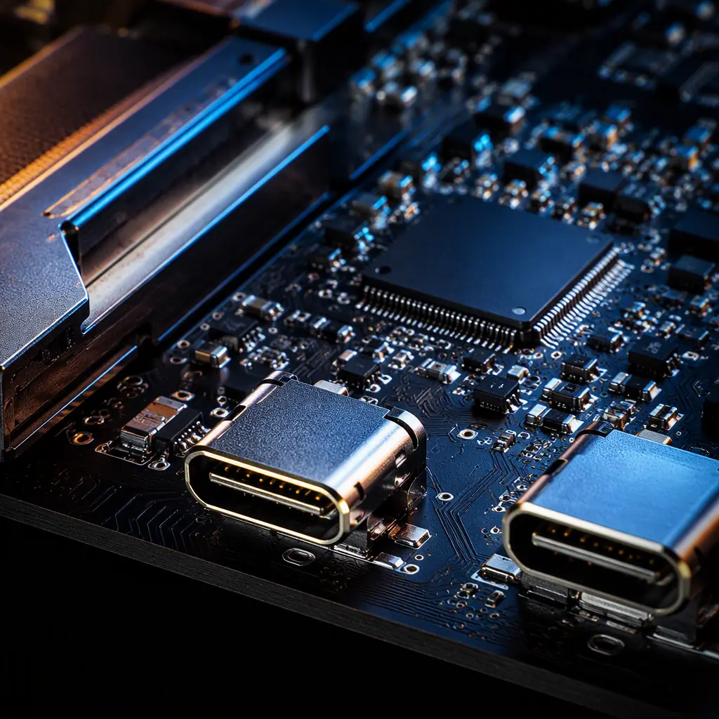
USB4 Gen4 (80 Gbps) and Thunderbolt 5 push 40 Gbps per lane over a differential pair on a board that may also route PCIe, DisplayPort, and 100 W of power delivery. At these speeds, the trace itself becomes a transmission line whose loss, crosstalk, and impedance discontinuities determine whether the link trains at full speed or falls back to 20 Gbps, or fails compliance entirely. The design rules that worked for USB 3.2 and PCIe Gen3 are no longer sufficient: at 40 Gbps per lane, a single via stub or a connector with 0.5 dB extra loss can consume the entire link budget.
This guide covers what a hardware team needs to specify and verify for a USB4/Thunderbolt board: the loss budget calculation, stackup and material selection, differential routing rules, re-timers and re-drivers (when and where), connector and cable selection, and the manufacturing tolerances that affect compliance. Huaxing PCBA fabricates boards up to 32 layers with ±5% impedance control and low-loss laminates (Isola, Panasonic, Rogers), and we see which designs pass 40 Gbps compliance and which do not. The differences are almost always in the first-pass layout, not the silicon. For the PCIe side of a USB4 link, our PCIe Gen4/Gen5 routing guide is the companion piece.
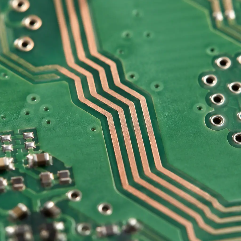
The USB4 Loss Budget: Where the Decibels Go
Every USB4/Thunderbolt link has a total insertion-loss budget allocated between the PCB, the connector, and the cable. For USB4 Gen3 (20 Gbps/lane) over a Type-C connection, the host-side PCB budget is typically around 3.5–4 dB at 10 GHz; at Gen4 (40 Gbps/lane) the budget tightens to roughly 2.5–3 dB at 20 GHz. Understanding where each decibel is spent is the first design task.
| Loss Contributor | Typical Budget (Gen3) | Typical Budget (Gen4) | How to Control |
|---|---|---|---|
| PCB trace (100 mm, FR-4) | 1.5–2.5 dB | 2.5–4 dB | Low-loss laminate, shorter run |
| Via transitions (2-4) | 0.3–0.8 dB | 0.5–1.2 dB | Back-drilling, via-in-pad |
| Type-C connector | 0.5–0.8 dB | 0.7–1.0 dB | Gen4-rated connector |
| AC coupling caps | 0.1–0.2 dB | 0.2–0.3 dB | 0402, low-ESR, matched pair |
| Total PCB budget | 3.5–4 dB | 2.5–3 dB | Sum must fit before cable |
Calculate your trace loss before you route
Use the laminate's Df (dissipation factor) and Dk at 10–20 GHz to compute loss per millimeter for your chosen stackup. Standard FR-4 loses roughly 0.2–0.3 dB/cm at 10 GHz; a mid-loss laminate (e.g., Isola I-Speed, Panasonic Megtron 4) loses 0.1–0.15 dB/cm; a low-loss material (Megtron 6, Rogers) drops below 0.08 dB/cm. If the controller-to-connector run is longer than 80–100 mm at Gen4, plan for a re-timer or a low-loss material from the start. Our laminate selection guide compares the material families.
Account for every via: stubs are silent budget killers
At 20 GHz, a 0.5 mm via stub has meaningful reflection loss. Back-drill every high-speed via to within 0.2 mm of the target layer, or use blind/buried via constructions so the signal never sees a stub. For 40 Gbps links, consider via-in-pad with copper fill on the connector and controller BGA breakout. Our back-drilling guide covers the process tolerances.
Key Takeaway: Do the loss-budget math before routing. If the total exceeds the budget on paper, no amount of layout heroics will save the link, change the material, shorten the route, or add a re-timer.
Stackup and Material Selection for 40 Gbps
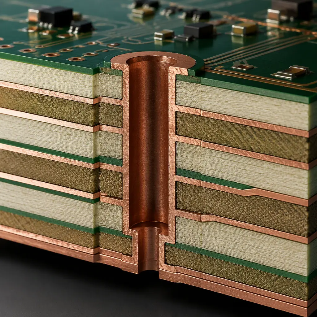
The stackup decision happens before schematic sign-off, because it determines the achievable impedance tolerance, the loss, and the cost. A USB4 board is typically 8–12 layers: the high-speed pairs live on two dedicated routing layers with a solid ground reference on the adjacent plane.
Reference plane discipline: adjacent ground, no splits
Every USB4 differential pair must have a continuous ground plane directly below it (one dielectric layer away). Never route pairs over a plane split, a cutout, or a different reference. The impedance discontinuity causes reflection loss that does not show up in the schematic, only in the compliance eye diagram. When a pair must change layers, add ground stitching vias beside the transition.
Impedance target: 85 Ω differential ±10%
USB4 specifies 85 Ω differential (with 90 Ω legacy compatibility) for the TX/RX pairs. Specify the impedance on the fab drawing and verify with TDR coupons on every panel. The ±10% tolerance is achievable with standard controlled-impedance processing; the tighter ±5% option costs more and is usually unnecessary unless the total loss budget is critical. See our impedance control guide for the coupon and verification workflow.
Material grade by link length and layer count
Short Gen4 runs (under 50 mm) can survive on FR-4 with careful layout. Runs of 50–150 mm need a mid-loss laminate. Anything longer, or any board with multiple Gen4 ports, should use low-loss material for the signal layers even if the rest of the stackup stays FR-4 (hybrid stackup). Specify the exact laminate part numbers in the fab notes. "low-loss" without a part number means the fab picks, and the fab will pick the cheapest.
Differential Pair Routing: The 40 Gbps Discipline
At 40 Gbps per lane, the physical routing rules are close to PCIe Gen5 and 100 GbE: tight coupling, matched lengths, minimal layer changes, and absolute avoidance of right-angle bends, stubs, and vias in the middle of the pair.
Pair geometry: edge-to-edge coupling, 5× spacing
Keep the two traces of a pair edge-to-edge (W/W = 1:1 or tighter) for strong coupling, and space pairs at least 5× the dielectric height from each other and from single-ended signals. At these speeds, crosstalk between adjacent pairs is a real budget item, our crosstalk analysis guide quantifies it.
Length matching: intra-pair ±5 mil, inter-lane ±100 mil
The two traces of a pair must be length-matched to ±5 mil (0.13 mm). A skew of 10 mil at 40 Gbps is measurable phase error. Between lanes (e.g., the four RX lanes of a Gen4 link), keep the total length spread under ±100 mil. Match lengths with serpentine bends only where there is room to keep the 5× spacing; a serpentine too close to its own pair ruins the coupling.
Breakout and connector area: the hardest part
The controller BGA breakout and the Type-C connector footprint are where most Gen4 designs fail. Use a proper escape pattern (dog-bone or via-in-pad) that keeps the pairs on the same layer as long as possible, place the AC coupling caps as 0402 with the pair routed straight through, and keep the connector's paddle-board or solder-tail region impedance-controlled. Our high-speed connector routing guide covers mezzanine and Type-C breakout patterns.
Re-timers and Re-drivers: When and Where

A re-timer (or re-driver) regenerates the signal in the middle of the link, effectively splitting the loss budget into two halves. It is the standard solution when the controller-to-connector distance exceeds the budget, or when the board must drive a long cable. The decision is architectural: adding a re-timer costs $3–8 in BOM and needs its own power and configuration, so you only add it when the math demands.
Where re-timers belong in a USB4 design
Put the re-timer between the controller and the connector, close to the connector (within 20 mm), so the high-loss segment is the connector/cable side. Each re-timer handles one or two lanes; a Gen3 x2 link needs one dual-lane device, a Gen4 x2 needs two or a quad device. Follow the vendor reference design for the configuration pins, I2C control, and the crystal/clock input, re-timers are clock-sensitive.
Re-timer vs re-driver: know the difference
A re-driver amplifies the signal but does not recover the clock; a re-timer fully regenerates the data with a local clock and clean edges. For USB4 Gen3/Gen4, use re-timers, not re-drivers. The equalization and clock recovery are required at 20+ Gbps. Re-drivers belong in lower-speed (USB 3.x, DisplayPort 1.4) designs.
Connector and Cable Selection
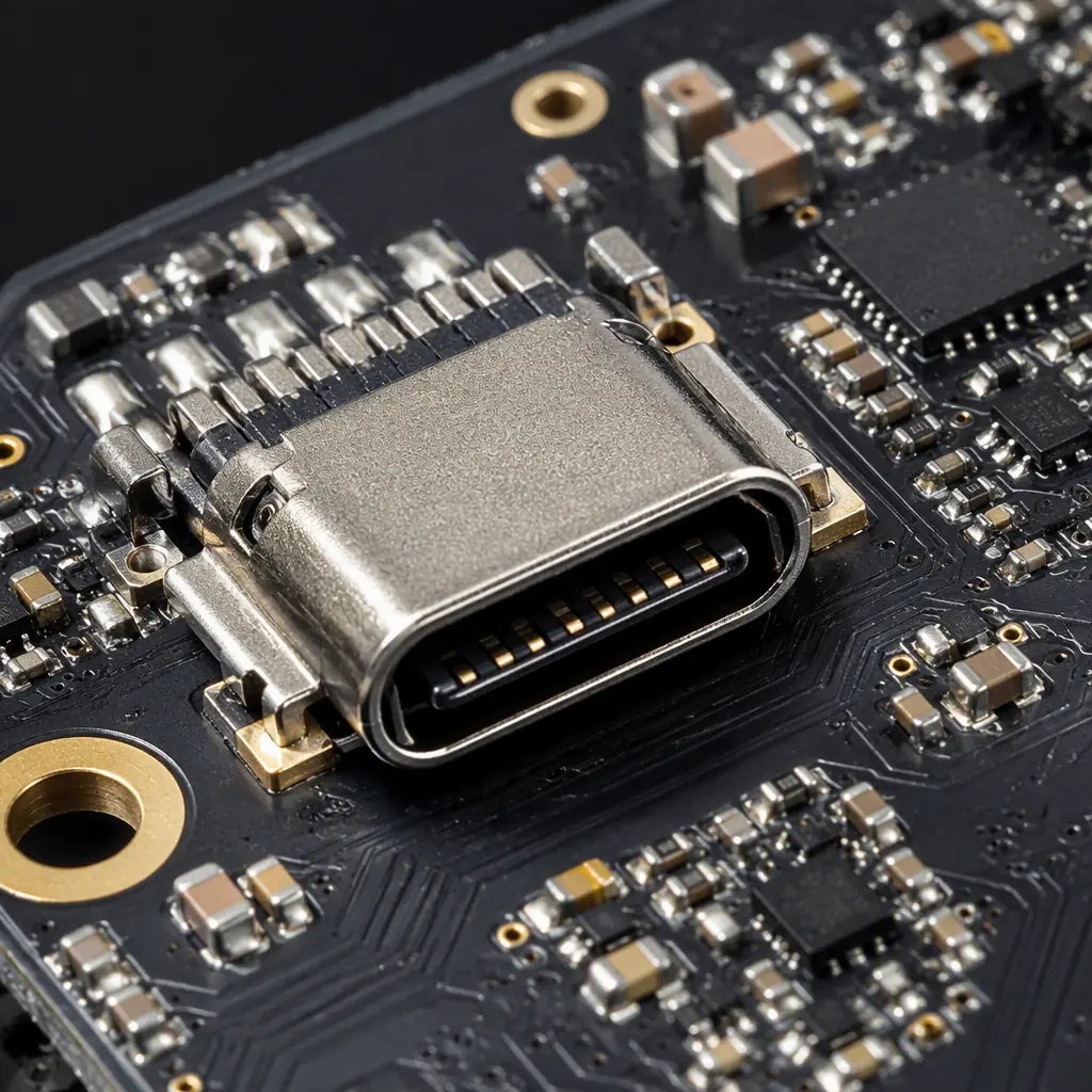
The Type-C connector is a mechanical and signal-integrity component at the same time. A connector rated for USB 3.2 (10 Gbps) will pass Gen3 data in many cases, but at Gen4 (40 Gbps) the connector's insertion loss and return loss become critical, and the connector's internal paddle card, if any, adds its own loss and impedance discontinuities.
Specify a Gen4/USB4-rated connector
Choose a Type-C connector whose datasheet states insertion loss and return loss at 20+ GHz, with a rated differential impedance of 85 Ω. Ask the vendor for the S-parameter model and simulate the connector footprint in your channel simulation, the connector is 20-30% of the total budget. Do not reuse a USB 3.2-era connector from a previous design without re-verifying its S-parameters.
ESD protection on the Type-C pins without killing the signal
Every external connector needs ESD protection, but a high-capacitance TVS on a 40 Gbps pair destroys the eye. Use low-capacitance (≤ 0.3 pF) TVS or diode arrays rated for the signal speed, and place them on the short stub between the connector and the series caps, never directly on the main trace. Our USB-C design guide covers the protection and power-delivery layout in full.
Procurement Tip: When you send a USB4 board to fabrication, the fab notes must specify: laminate part numbers, impedance targets with TDR coupon verification, back-drilling depth tolerance, and surface finish (ENIG or ENEPIG for the connector pads). A vague fab note is how a 40 Gbps board comes back at 20 Gbps.
Manufacturing Verification: What to Demand From the Fab
High-speed boards are only as good as the manufacturing verification behind them. Three checks make the difference between a compliant product and a paperweight: impedance coupons, back-drill accuracy, and surface finish consistency.
TDR impedance coupons on every panel
Require a TDR test report for the controlled-impedance nets on every production panel, not just the first article. The report must show measured differential impedance within ±10% of 85 Ω. Our impedance guide includes a sample coupon layout you can copy.
Back-drill verification by cross-section
Ask for a cross-section photo of a back-drilled via on the first article showing the remaining stub length. The spec is typically "stub ≤ 0.15–0.2 mm after back-drill", verify it once, then spot-check on later batches. See our cross-section report guide for how to read the photos.
Surface finish: ENIG/ENEPIG for the connector area
Type-C connector pads and the high-speed breakout area should be ENIG (or ENEPIG if the board also carries wire-bonded or high-mating-cycle contacts). HASL's uneven surface is a signal-integrity and planarity problem at 40 Gbps. Our surface finish selection guide compares the options.
Designing USB4 Boards That Pass Compliance
The pattern in every successful USB4 design is the same: a loss budget written before routing, a stackup chosen to meet it, pairs routed with the discipline of a 100 GbE backplane, and manufacturing verification that treats impedance as a specification rather than a hope. Do that and the compliance test is a formality; skip any step and the debug happens on a $50,000 scope with the tape-out clock ticking.
At Huaxing PCBA, we fabricate USB4, Thunderbolt, and PCIe Gen5 boards up to 32 layers with low-loss laminates, ±5% impedance control, back-drilling, and ENIG/ENEPIG finishes. Send us your stackup and routing files for a manufacturability review. We will validate the impedance targets, via construction, and back-drill requirements before you commit to tooling. Contact our engineering team, or continue with our signal integrity design guide for the broader high-speed picture.
