A printing defect is the cheapest defect in electronics assembly to prevent and the most expensive one to leave alone. It is created in under two seconds, on a single station, by a process whose variables are almost entirely controllable. It is also the defect that propagates furthest: the same thin deposit becomes an open joint after reflow, an intermittent connection after thermal cycling, and a field return after six months in a customer's enclosure. Between those two ends sits the entire economics of an SMT line.
Most of the printing-defect literature is diagnostic. It tells you that insufficient paste comes from an area ratio below 0.66, that bridging comes from too much paste volume or too little separation speed, and that slumping comes from a paste held open past its working time. All of that is useful and none of it is a business case. A buyer cannot approve a GBP 60,000 printer on the strength of a defect atlas. A process engineer cannot win an argument about stencil coating with a photograph.
What follows is the money side. What a printing defect costs at each point in the line where it can be caught, why the detection point matters more than the defect type, how to build a cost model on your own volumes, and which four levers actually move printing yield. The diagnostic order for the defects themselves is covered separately in solder paste printing defects, and this page assumes you have already identified which defect you are looking at.
What a Printing Defect Actually Costs
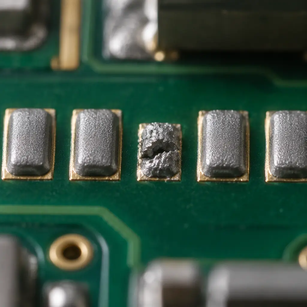
A starved deposit is the same defect at SPI as it is at rework. Only the cost changes, and it changes by an order of magnitude.
The instinct is to price a defect as the value of the component it affects. That is the smallest part of the number. A printing defect carries five separate costs, and which of them you actually pay depends entirely on where the defect is caught.
Material cost is the first and least significant. The component that must be replaced, the paste that must be re-printed, the board if it cannot be cleaned. On a typical mixed-technology industrial board the component is often under a dollar and occasionally over twenty, which is a wide spread but still not what decides the argument.
Labour cost is the second. Rework is manual by definition, and manual work scales with the number of joints being touched rather than with the number of boards. A 0402 resistor replaced by a skilled operator is a minute. A BGA on a fine-pitch board that must be removed, the site dressed, new paste printed through a mini stencil, re-placed and reflowed, then X-rayed, is fifteen to thirty minutes plus an oven or hot-air cycle, and it carries its own risk of collateral damage to neighbouring parts. Repairs also consume a rework operator who is not available for anything else.
Test cost is the third and it is almost always under-counted. A defect that survives printing is caught by test equipment you have already paid for: SPI if you have it, AOI after reflow, ICT or flying probe on the finished board, functional test at the end. Testing a defective board is not free even though the test itself was budgeted, because the failure triggers a diagnostic step, a disposition decision, and usually a second pass through the test cell after rework.
Capacity cost is the fourth and the hardest to see. Every board that goes through rework occupies a slot on a line that could have been producing a good board. On a line running three shifts at capacity, rework is not a cost, it is a throughput loss, and the throughput loss is priced at the contribution margin of the product, not at the cost of the repair.
Field cost is the fifth, and it is the one that ends supplier relationships. A printing defect that escapes every electrical test is usually one that makes intermittent contact: a component sitting on a deposit too thin to form a reliable fillet, passing continuity at the factory, opening under thermal cycling three months later. Field failure cost includes the return logistics, the diagnosis, the replacement, the labour at the customer site, the administrative cost of the complaint, and the implicit cost of the next purchase order going to someone else.
| Caught at | Typical cost per event | Who pays | What it consumes |
|---|---|---|---|
| SPI, before reflow | Wipe and re-print, under a minute of line time | Assembler, invisible in the quote | Paste, one board cycle |
| Post-reflow AOI, before test | 15-45 minutes of rework labour plus component | Assembler | Rework station, an operator |
| ICT or flying probe | Rework labour plus a second test pass | Assembler | Rework plus test cell capacity |
| Functional test | Rework plus diagnosis engineering time | Assembler | Engineering hours, test cell, schedule |
| Customer incoming or field | Return freight, replacement, site labour, complaint handling | Shared, and the relationship | Warranty reserve, credibility |
Two things follow from that table. First, the cost of a defect is not a property of the defect, it is a property of the detection point, and the multiplier between the first row and the last is commonly between ten and forty. Second, the cheapest intervention is not a better printer or a better stencil, it is catching the defect earlier, which is why SPI pays for itself on high-mix work even when the defect rate is already low.
Key takeaway: Do not budget printing defects by component value. Budget them by where you catch them. Moving the average detection point one stage earlier is usually worth more than halving the defect rate.
The Defect Classes That Carry Real Money
Printing defects are usually listed alphabetically in textbooks and by frequency in production reports. Neither ordering is useful for costing, because frequency and cost are only loosely related. A defect class that happens constantly but is caught by SPI within seconds is a process annoyance. A defect class that happens rarely but produces a latent open is a warranty problem. Sorting by how the defect fails rather than by how it looks is the only ordering that prices correctly.
Insufficient paste is by far the most common and, in cost terms, the most benign when SPI is in place. A starved deposit on a fine-pitch pad produces a weak fillet, which AOI flags and rework fixes. The money case against it is not the rework, it is the false calls it generates on SPI and the fact that a marginal deposit that passes SPI limits can still become an intermittent joint. Where insufficient paste becomes expensive is on thermal pads and on ground-plane connections, where a partial deposit creates a void that only shows up in X-ray or in thermal performance.
Bridging is the defect with the best cost profile, because it is nearly always visible and nearly always caught. Paste bridging between adjacent pads is obvious at SPI and obvious at AOI, and it is cheap to fix before reflow. The exception is bridging under a component body where AOI cannot see, at which point it becomes a short that ICT catches and that may have already damaged a component or a power rail. Bridging under a BGA or a connector body is where a cheap defect becomes an expensive one.
Slumping and solder balling sit in the middle. Slumped paste spreads during the soak phase and can produce bridges or beads that are cosmetic at Class 2 and rejects at Class 3. Solder beading, where a small sphere forms beside a chip component, is one of the most persistent and least understood printing-related defects, and it is expensive mainly because it is intermittent: it depends on paste volume, aperture shape, stencil separation and the oxidation state of the paste in a way that makes it resistant to a single-parameter fix.
Misalignment is cheap when it is small and expensive when it is systematic. A slight offset on a 0402 that still forms a fillet is a non-event. An offset that walks over a reflow profile to produce a tombstone is a rework event, and a stencil that has drifted relative to the board datum will produce that offset on every board in the lot until someone measures it.
Paste on the solder mask, paste smear on the board edge and paste on gold fingers are the cosmetic classes. They cost nothing in function and everything in a Class 3 or medical build, where a contaminated edge connector is a reject regardless of whether it would have worked. Buyers who specify Class 3 acceptance while running a printing process tuned for Class 2 volume are buying rejects, not quality.
A Worked Cost Model You Can Run On Your Own Numbers
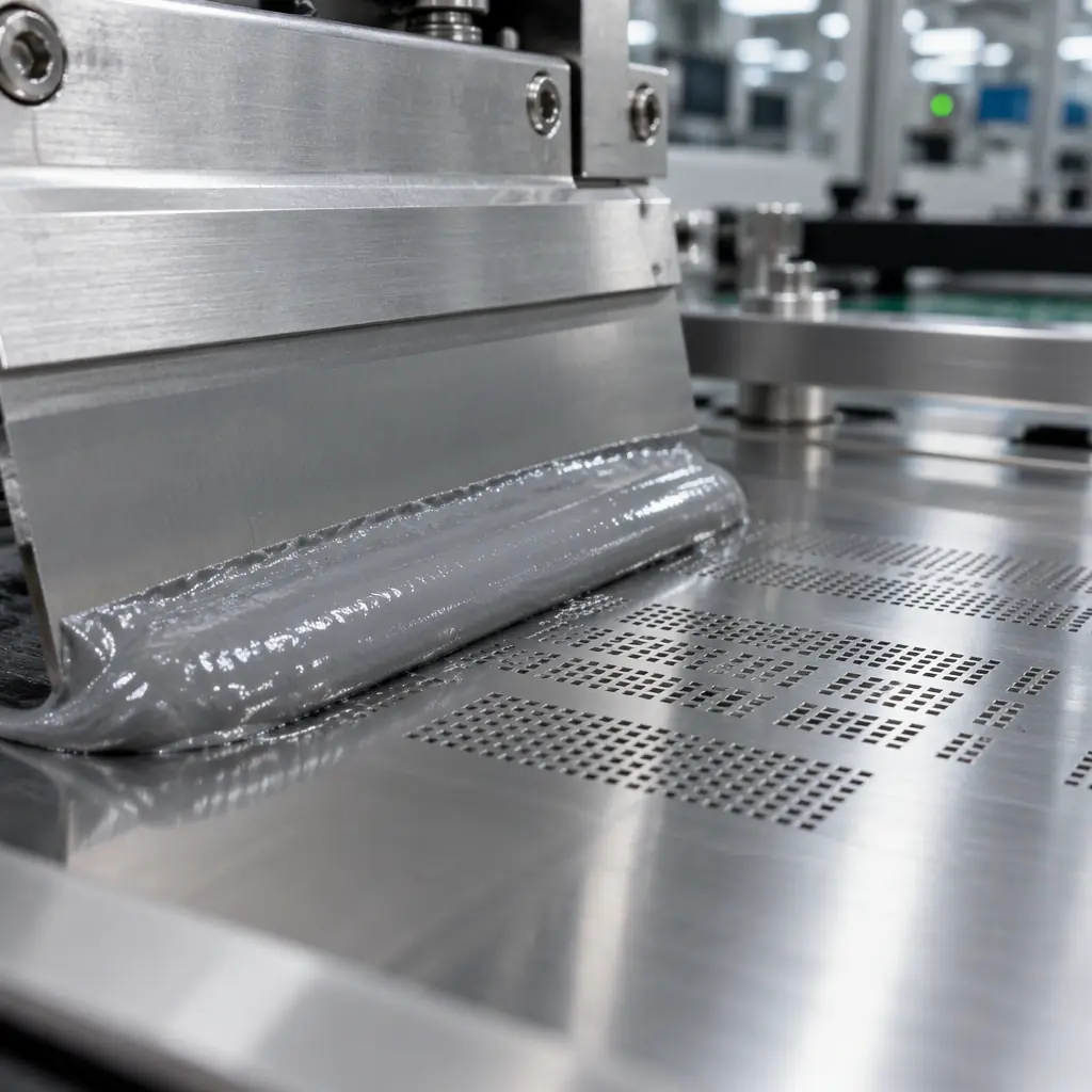
The printing station is the smallest capital item on the line and the cheapest place to remove cost from a build.
The model below takes six inputs, all of which a buyer can obtain from a supplier or from their own line. It is deliberately arithmetic rather than statistical, because the purpose is to decide whether an intervention pays, not to forecast a defect rate.
| Input | What it means | Where to get it |
|---|---|---|
| Annual volume N | Boards assembled per year on the line | Your forecast |
| Printing DPPM d | Defective joints per million after printing, before inspection | SPI data, or AOI-derived estimate |
| Joints per board j | Total printed joints including passives | BOM and court count |
| Cost per detected defect c | Rework labour plus component plus test re-pass | Your rework log |
| Escape fraction e | Share of defects that pass all test stages | Field return rate, or 1-5% estimate |
| Cost per escape f | Field failure cost including logistics and labour | Warranty data |
Annual defect cost is then the detected defects multiplied by the detection cost, plus the escaped defects multiplied by the field cost. Detected defects per year are the annual volume multiplied by joints per board multiplied by the defect rate per million, divided by a million. Escaped defects are that result multiplied by the escape fraction.
Run it at two volumes with realistic mid-range numbers for an industrial control board with 800 joints, a printing defect rate of 400 DPPM, a rework cost of USD 18 per detected defect, an escape fraction of 2 percent and a field cost of USD 400 per escape. At 5,000 boards per year the line produces 1,600 defective joints, of which 32 escape. Detected cost is USD 28,000 and field cost is USD 12,800, for a total of roughly USD 41,000 a year. At 50,000 boards the same numbers give USD 410,000. The defect rate is identical and the business impact differs by a factor of ten.
Now price an intervention. A nano-coated stencil with a tight area-ratio design typically moves printing DPPM by 30 to 50 percent on fine-pitch work, at a tooling cost of a few hundred dollars per stencil per design revision. At 5,000 boards that intervention is worth USD 12,000 to 20,000 a year against a tooling cost in the low hundreds, which is not a close call. An automatic printer with closed-loop SPI feedback does better still, but it carries a capital cost in the tens of thousands and a floor-space cost, so the break-even volume matters: at 2,500 boards a year with a 400 DPPM baseline, a printer costing USD 60,000 never pays back on defect cost alone, and must be justified on changeover time, NPI speed and operator dependence instead.
There is a third break-even worth computing, because it is the one that changes supplier decisions: the volume at which in-line SPI becomes cheaper than the field failures it prevents. If SPI reduces the escape fraction from 2 percent to 0.5 percent, the saving is 1.5 percent of defective joints multiplied by the field cost. At the numbers above, at 5,000 boards a year, that is 24 escapes avoided at USD 400, or USD 9,600 a year, which has to be compared with the cost of the SPI system and its programming labour. The honest answer for a 5,000 board a year build with a competent printer is that SPI is a quality-assurance decision rather than a cost-saving one, and buyers should be told that rather than sold a saving that does not exist.
Key takeaway: At low volume, stencil and paste discipline return money fastest because the tooling cost is small. At high volume, printer capability and in-line inspection win because every percentage point of yield is multiplied by a large number of boards.
Where the Money Is Actually Lost: Detection Point, Not Defect Type
The single most useful number in printing economics is the multiplier between what a defect costs when it is caught at SPI and what it costs when it escapes. On a typical fine-pitch industrial build that multiplier is between twenty and forty, and it is driven by four things that get worse at every stage: the diagnostic effort rises, the rework difficulty rises, the capacity consumed rises and the risk of collateral damage rises.
At SPI, the cost of a defect is a wipe and a re-print. The board has no components on it, so there is nothing to damage and nothing to remove. The line loses a few seconds. The only real cost is the false-call rate of the SPI itself, because a system tuned to catch every marginal deposit will stop the line on good boards, and every stop has a cost. This is the trade-off that SPI recipe tuning is really about: a limit tight enough to catch the latent opens and loose enough that the line is not stopped by good product. The economics favour tight limits on fine-pitch apertures and looser limits on large thermal pads, because the consequence of a marginal deposit is not the same on both.
At AOI, the board has been through reflow. The defect is now a physical joint, the component is attached, and fixing it means removing and replacing. Rework on a finished board carries a risk that did not exist before reflow: a hot-air cycle that lifts an adjacent component, a wicking problem on a thermal pad, flux residue that must be cleaned under a low-clearance part. AOI is a necessary net, but it is a net that catches a much more expensive defect than SPI does.
At ICT or flying probe, the board is electrically complete and has often been through a second reflow for the bottom side. A failure here is ambiguous: the test tells you a node is open or shorted, not which joint caused it. Diagnosis consumes engineering time, and the rework is performed on a board that already has both sides populated, which makes access worse and reflow risk higher.
At functional test, the board has passed electrical continuity and failed on behaviour. The failure could be a printing defect, a placement error, a wrong component, a firmware issue or a genuine design margin problem, and separating those cases is engineering work, not operator work. This is the stage where the cost per defect turns from operator minutes into engineer hours.
The practical consequence for a buyer is that inspection strategy is not a quality expense to be negotiated down, it is the main determinant of who absorbs the cost of printing variation. A supplier who runs SPI and a supplier who runs only AOI can quote the same per-board price and deliver very different total costs, and the difference appears in the buyer's own field return data a year later.
The Four Levers That Move Printing Yield
Printing yield is set by four subsystems, and improvements are cumulative rather than substitutable: a perfect stencil on a badly aligned printer produces the same defects as a bad stencil on a perfect printer. The ranking below is by return on effort, which is not the same as by capital cost.
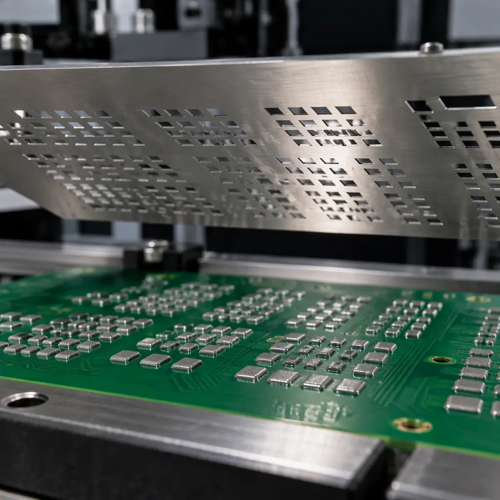
The first lever is the stencil, and within the stencil the aperture area ratio is the governing variable. Area ratio is the aperture opening area divided by the aperture wall area, and below roughly 0.66 paste release becomes unreliable regardless of everything else. A design that needs a 0.4 mm pitch aperture on a 0.12 mm foil is at the edge of what a laser-cut stencil will release consistently; the same design on a 0.10 mm foil, or with a nano-coating that reduces paste adhesion to the wall, releases reliably. Foil thickness, aperture shape and wall finish are the three stencil variables that matter, and all three are cheap to change at tooling time and expensive to change after a build is released. The design rules are set out in SMT stencil aperture design.
The second lever is the paste. Rheology determines how a deposit behaves between printing and reflow: whether it holds its shape, whether it slumps during the soak phase, how it releases from the aperture wall, and how much it absorbs water from the air. Paste that has been open past its working time thickens, releases poorly and slumps less predictably, which produces a defect pattern that moves through the shift. Paste that has been stored badly or used past its shelf life behaves the same way even if it was never opened. The behaviour itself is covered in solder paste rheology, and the handling rules in solder paste shelf life.
The third lever is the printer itself: alignment repeatability, squeegee pressure and speed, separation speed, and board clamping. These are the variables that produce systematic rather than random defects. A printer with 25 micron repeatability will hold a fine-pitch aperture centred; a printer with 50 micron repeatability will not, and the resulting offset is invisible on coarse pitch and fatal on a 0.4 mm part. Squeegee speed and pressure determine paste roll quality and how much paste is pushed through the aperture; separation speed determines whether the deposit is pulled out of the aperture cleanly or torn.
The fourth lever is inspection and feedback. SPI is only worth its cost if its results close the loop, meaning that the data is used to adjust printer parameters and not just to reject boards. An SPI system that reports a rising trend in paste volume on one aperture and does nothing with the information is a very expensive reject gate. Where the loop is closed, SPI is also the tool that proves whether a stencil change or a paste change actually worked, which is what turns process improvement from opinion into measurement. How SPI, AOI and X-ray divide the work is covered in AOI, X-ray and SPI inspection.
Where those four levers are not enough, the alternative is to remove printing from the process entirely for the affected build. Solder paste jetting deposits paste without a stencil, which makes it viable for prototypes, for boards with very few joints and for builds where the stencil tooling lead time is the bottleneck. It is not a drop-in replacement for high-volume stencil printing on cost, and the comparison is set out in solder paste jetting versus stencil printing.
What to Ask a Supplier Before You Award the Build
Printing capability is one of the few areas where a supplier's answers are diagnostic. The questions below are chosen so that a supplier who has real process control answers them with numbers, and a supplier who is quoting a capability they do not have answers them with adjectives.
Ask what printing defect rate they measure and against what baseline. A supplier with SPI can quote a DPPM figure and a trend. A supplier without SPI can only quote a final yield, which conflates printing with placement, reflow and component quality. Ask whether the SPI data is retained per lot and whether it is available to the customer on request; retention is the difference between process control and process theatre.
Ask what the minimum area ratio in their standard stencil process is and what foil thickness they default to for fine-pitch work. The answer should describe an area ratio limit and a rationale, not a pitch figure. Ask whether nano-coated stencils are standard or an upgrade, and whether the coating is applied to the aperture walls or only the surface, because the surface-only treatment does much less for paste release.
Ask how they handle paste open time and what happens to a paste cartridge at the end of a shift. The good answer describes a working-time limit per print session, a documented discard or return rule, and a storage regime with temperature logging. The weak answer is that paste is used until it runs out.
Ask what their rework cost per defect is and where the rework station sits in the flow. The answer tells you whether they count rework as a cost or absorb it silently, and whether reworked boards re-enter test. Ask whether reworked boards are marked in the lot record, because a supplier who cannot tell you which boards were reworked cannot tell you their real first pass yield.
Ask what they do when a printing trend moves on a running lot. A supplier who stops the line and re-qualifies the stencil or the paste has a process. A supplier who increases inspection and ships has a hope. The first is worth paying for; the second is worth avoiding, because the cost of their hope becomes your field data. First pass yield discipline as a whole is covered in SMT first pass yield improvement, and the acceptance standards that decide whether a marginal deposit is a reject are set out in IPC-A-610 acceptance criteria.
Putting a Number on Printing
Printing defects are the cheapest defects in the plant to prevent and the most expensive to inherit. The cost of a defect is set almost entirely by where it is caught, and the multiplier between SPI and field across a typical fine-pitch build is large enough that inspection strategy, not defect rate, is the first thing a buyer should examine. On any build where printing variation can produce a latent open, the useful question is not what the defect rate is but what the escape rate is, and whether the supplier can measure it.
At Huaxing PCBA printing is run with laser-cut stencils to a 0.66 minimum area ratio, nano-coated aperture walls on fine-pitch builds, and in-line SPI with per-lot data retention. Paste is controlled by working time per session with logged storage, and reworked boards are recorded against the lot so that first pass yield is a real number rather than a reported one. If you have a build where printing defects are showing up in your own yield data and you want to know which stage of the process is producing them, send the defect images and the SPI or AOI export through the quote form and we will map the pattern to a cause and a cost.