
Every high-speed server board arrives at the same decision point, and it arrives earlier than most teams expect: the connector is chosen before the stackup, and from that moment the PCB's freedom is mostly gone. A 112 Gbps PAM4 backplane connector does not simply plug into a board. It dictates a hole diameter with a tolerance band a few hundredths of a millimetre wide, a via-stub budget that removes most of the routing layers, an impedance target that constrains both laminate choice and trace geometry, and an escape pattern that has to resolve a 0.8 mm contact pitch down to a 0.9 mm BGA pitch inside the first two layers.
Most of the published guidance covers the routing response: stackup, loss budget, crosstalk, equalisation. That is the second half of the problem. The first half is what the connector requires, in numbers, before a route exists. Those requirements belong on the fabrication drawing, not in the routing notes, because they are the ones that fail in production after the design is locked.
This page works through five connector families and the PCB parameters each one forces, with the numbers that break first. For the routing and stackup side, the companion guide on high-speed connector PCB design covers loss, crosstalk and simulation.
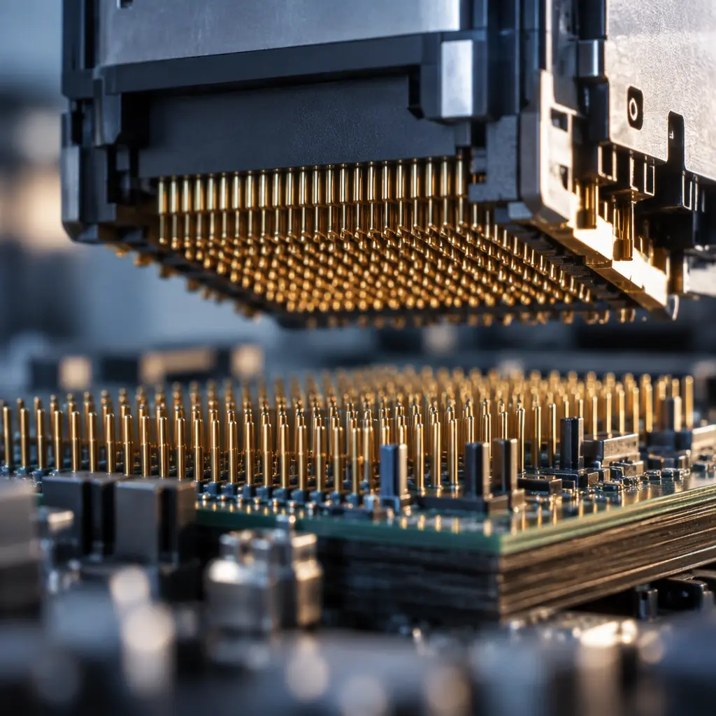
What the Connector Forces Onto the Board
Five hand-offs happen between a connector datasheet and a fabrication drawing. Each one is a constraint the PCB has to absorb, and each one has a characteristic failure mode on a server board.
Hole geometry. Compression-fit contacts specify a finished hole diameter of typically 0.46 mm to 0.60 mm with a specific tolerance band, plus a maximum hole-size distribution across the pin field. The band is usually 0.05 mm total, i.e. finished diameter, not drill diameter, which means plating thickness tolerance is inside the band. This is the single most common source of press-fit failure.
Via stub. At 56 Gbps PAM4 the acceptable stub on a through-hole layer transition is around 0.3 mm; at 112 Gbps it approaches zero, and backdrilling becomes mandatory on every signal via in the connector escape. That converts a 6-layer decision into a backdrill-depth tolerance on a 20+ layer board, which is where cost and yield diverge.
Impedance and laminate. Connector-rated channels are specified as a 100 Ω differential system with loss targets per inch. That draws a line from the connector through the stackup: at 112 G, conventional FR-4 will not carry the loss, and the connector escape region ends up on a low-loss laminate while the rest of the board stays on high-Tg FR-4 — a hybrid stackup with its own registration and thermal-expansion issues.
Escape density. A high-speed backplane connector presents contacts at 0.8 mm or 1.0 mm pitch, often in a staggered four- or six-row pattern. Getting those signals to a 0.9 mm BGA escape within the first two signal layers consumes most of the available routing width, which is why connector-adjacent regions become the densest part of the board and the first place DRC and yield problems appear.
Thermal mass. A 400-pin press-fit connector is a large metal block attached to the board. During reflow it draws heat out of adjacent joints; during repair, it withstands a limited number of insertion cycles. Both effects have to be reflected in the assembly process, not just the layout.
What PCB Requirements Do High-Speed Server Connectors Impose?
Short answer, for the search snippet: High-speed server connectors impose five PCB requirements: a finished hole diameter with a total tolerance band of roughly 0.05 mm for press-fit contacts, a via-stub limit of 0.3 mm at 56 Gbps and near-zero (backdrilled) at 112 Gbps, a 100 Ω differential impedance with a defined loss budget per inch, an escape pattern that resolves connector pitch to BGA pitch within two signal layers, and thermal management for the connector's mass during reflow and rework.
The matrix below turns those five into per-family numbers. Values are typical for current production parts; each connector family has its own datasheet tolerance, and the datasheet always wins. What the table is for is knowing which question to ask.
| Connector Family | Typical Rate | Hole Requirement | Stub Limit | Dominant Failure Mode |
|---|---|---|---|---|
| Backplane header / receptacle (compression-fit) | 25-112 G PAM4 | 0.46-0.60 mm finished, ±0.025 mm | <0.3 mm at 56 G; backdrill at 112 G | Hole size drift out of band → retention force below spec |
| Mezzanine board-to-board | 25-56 G | SMD pads, 0.5-0.8 mm pitch | Controlled by stackup choice | Coplanarity and solder wicking on fine-pitch pads |
| Cable-backplane / twinax assembly | 56-112 G | SMD pads + mechanical mounting holes | <0.2 mm at 112 G | Pad-to-trace transition impedance discontinuity |
| Card-edge / gold-finger | 10-56 G | Bevel geometry, 0.05 mm plating | n/a (edge launch) | Bevel depth and contact wear over mating cycles |
| Co-packaged / socketed optics | 112 G+ | Socket pad grid, <0.5 mm | Near zero on escape vias | Socket contact resistance and thermal creep |
Two rows deserve expansion, because the failures are expensive and slow to surface: press-fit hole tolerance, and via stub on backdrilled signal layers. Both sections below quantify the cost of getting them wrong.
For the retention-force side of the same problem, the specifications, acceptance criteria and pull-test numbers are in the press-fit retention and pull force guide; the assembly sequencing implications are in press-fit connector assembly.
Press-Fit Hole Tolerance and What It Costs When It Drifts
A compression-fit contact works by deforming the plated hole wall. The eye of the needle compresses as it enters, and the elastic recovery of the barrel creates the retention force. That mechanism depends on the finished hole diameter being inside a band that is narrow by PCB standards.
Typical requirement: 0.50 mm ±0.025 mm finished. Note the word finished. The drill is typically 0.55-0.60 mm, and plating reduces it by 50-100 µm depending on the target copper thickness in the barrel. On a 4.0 mm thick backplane, achieving 25 µm copper in a 0.55 mm hole means plating for a long time in a high-aspect-ratio hole, and plating distribution across a 400-hole connector field is never perfectly uniform.
| Deviation | Immediate Effect | When It Surfaces | Recovery Cost |
|---|---|---|---|
| Hole 0.02 mm under minimum | Insertion force above tooling limit; contact may buckle | Assembly, immediately | Scrap connector + possible board damage from extraction |
| Hole 0.03 mm over maximum | Retention below spec; contact still inserts normally | Vibration, thermal cycling, or field shock | Rework or scrap, discovered months later |
| Wide distribution across field | Mixed forces; some joints marginal, some fine | Qualification pull test on a sample, if sampled properly | Entire board population suspect |
| Barrel copper below spec | Retention fine, but barrel cracks under press-in stress | Thermal cycling (IPC-6012 class 3 microsection) | Whole lot, no field remedy |
The second row is the dangerous one. An oversized hole does not announce itself: the connector presses in, the board tests fine, and the joint goes marginal under thermal cycling. Server equipment sees exactly those conditions — inlet temperatures cycling with load, fans and chassis vibration. A board that passes first-article inspection on a good day can still be a field return six months later.
The countermeasure is measurement discipline, not tighter words: a completed-hole-size report per panel measured with a pin gauge or optical CMM on a defined sample across the pin field, with the mean and full range reported, not just conformance. A mean of 0.502 mm with all points in band is a different risk from a mean of 0.502 mm with a 0.048 mm range, in which the extremes are within a few microns of the limits and the next panel will step out.
Via Stub, Backdrilling and the Loss Budget at 56G and 112G
A through via on a 4.0 mm backplane creates an unterminated stub below the layer where the signal enters. At low frequency the stub is invisible. As the data rate rises, the stub becomes a quarter-wave resonator: it produces a notch in the insertion-loss curve whose frequency falls as the stub lengthens, and a peak in return loss that degrades the eye at the top of the band.
| Signal Rate | Nyquist Frequency | Practically Tolerable Stub | Typical Mitigation |
|---|---|---|---|
| 25 G NRZ | 12.5 GHz | 1.0-1.5 mm | Layer assignment on a thin board; no backdrill often acceptable |
| 56 G PAM4 | 14 GHz (28 GBd) | 0.3-0.5 mm | Selective backdrill on connector escape vias |
| 112 G PAM4 | 28 GHz (56 GBd) | <0.2 mm (≈0) | Backdrill all signal vias in channel; blind/buried via stackup |
Backdrilling has its own tolerance problem, and it is where the cost sits. The drill removes the unused barrel from the opposite side, stopping short of the target layer by a controlled depth. That depth tolerance is typically ±0.15-0.25 mm on a production backdrill, because the drill depth is referenced to the panel surface and the panel thickness itself varies. Too shallow leaves a stub; too deep damages the target-layer pad and the barrel above it.
Three consequences worth writing into the fabrication drawing:
1. Nominal board thickness with a tolerance, stated with the reference points. Backdrill depth tolerance and board thickness tolerance are coupled. If thickness varies ±0.13 mm across a panel and the backdrill is referenced to the surface, the effective stub varies by the same amount before the drill's own tolerance is applied.
2. Which vias are backdrilled, stated by net class, not by layer. Blanket backdrilling of a 20-layer server board removes copper that was holding thermal spreading and can affect controlled-impedance propagation in ways that only show up on TDR coupons. The layers, net classes and allowable residual stub belong on the drawing.
3. Coupon-based verification, before scrap rates climb. The impedance coupon route, measurement setup and acceptance band are covered in impedance test coupons and TDR; stub-specific verification uses the same coupons with a stub-length measurement. The backdrill process parameters themselves are detailed in our backdrilling guide.
On a 112 G design, backdrilling all signal vias in the connector escape can add a meaningful fraction to the fabrication price of a 20+ layer board, and it is the item most often value-engineered out during cost review. Removing it does not save the cost; it moves it to the link margin, where it appears as a non-functional board at system bring-up, with the schedule consequence that implies.
Escape Routing: Connector Pitch vs BGA Pitch
The connector and the BGA usually sit close together on a server board, and the two pitches almost never match. A backplane header at 0.8 mm staggered contact pitch, four rows deep, presents eight signals per 3.2 mm column pair. A 0.9 mm BGA with a 40 × 40 field presents one escape channel per 0.9 mm of depth per layer.
On a 100 Ω differential pair needing roughly 0.25 mm of trace-and-space per pair, the arithmetic usually resolves to one differential pair escaping per two BGA rows per signal layer. With three signal layers available in the connector-adjacent region after ground and power, that is six pair-channels for a field that may need twelve. The shortfall is resolved one of three ways, and each has a consequence:
| Resolving Option | Effect on Density | Effect on Signal Quality | Effect on Cost |
|---|---|---|---|
| More signal layers (thinner / more laminate) | Solves the arithmetic | Neutral if stackup is symmetric | Layer count and layer-pair registration cost |
| Any-layer HDI vias in the escape region | Adds escape channels per layer | Shortens stubs, generally improves | Highest fabrication cost of the three, concentrated in one area |
| Reduce pair count through the connector | Fits existing layers | Neutral | Cheapest, but reduces channel count — an architecture decision, not a layout one |
The important point is that this arithmetic has to happen before the stackup is frozen. Teams that discover the shortfall after the stackup is built usually take the third option under schedule pressure, then discover the channel-count reduction at system integration. The connector selection, the stackup and the escape strategy are one decision, not three.
What to Put on the Fabrication Drawing
The items below are the ones that separate a board that assembles reliably from one that produces a slow, expensive campaign of joint failures. They are all inexpensive to state and expensive to omit.
| Drawing Item | What To State | Why It Matters |
|---|---|---|
| Finished hole size | Diameter and tolerance for the connector pin class, marked as finished, with the measurement method | Drill size alone does not control retention; plating tolerance is inside the band |
| Hole size report | Per-panel sample plan across the pin field, mean and full range reported | Conformance alone hides the distribution that will drift on the next panel |
| Backdrill schedule | Net classes, layers, residual stub maximum, depth reference surface | Blanket backdrilling affects thermal and impedance behaviour outside the channel |
| Stackup with tolerance | Per-layer dielectric thickness and overall board thickness tolerance | Backdrill depth tolerance is coupled to thickness tolerance |
| Impedance coupons | Coupon location, target and tolerance per net class, TDR report required | The channel is only verified if it is measured on the same panel |
| Press-fit assembly note | Insertion force range, tooling, maximum re-insertions, flatness support | An otherwise perfect board can be destroyed at assembly |
| Connector revision lock | Exact connector part and revision, with change notification required | A connector revision changes the hole requirement; nobody re-checks the drawing |
The last row is the one that ages worst. A server platform runs for years, the connector vendor revises a contact geometry, the part number stays the same or the substitute is "equivalent", and the finished-hole requirement on the drawing no longer matches the contact now being inserted. The board that passed qualification at launch is not the board shipping in year three — the same logic as the change-notification clause in the fixture ownership analysis, applied to the mechanical interface rather than the test interface.
Server boards carry the highest layer counts and the tightest tolerances in volume PCB production, which is why the connector interface is where supplier capability is genuinely tested. Layer counts up to 32, backdrilling with a stated residual-stub limit, press-fit assembly with measured insertion force, and 100 Ω differential control with TDR verification per panel are the four capabilities the interface depends on, and they are the ones worth auditing before the connector is ordered rather than after.
For the system-level context — how the connector interface fits with the rest of a server board's power, thermal and backplane architecture — see data center server PCB and 112G and 224G SerDes PCB design.