
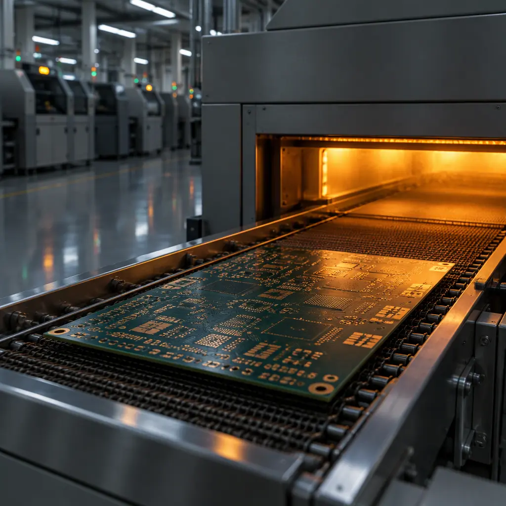
A mixed-technology board — one carrying both surface-mount devices and through-hole connectors — has traditionally meant two soldering processes. The SMDs go through reflow, then the connectors are added by wave soldering, selective soldering or hand soldering. Pin-in-paste, also called paste-in-hole, PIP or intrusive reflow, collapses that into a single reflow pass: the stencil is designed to deposit enough paste to fill the plated through-hole barrels as well as wet the SMD pads, the connectors are placed before reflow, and the whole assembly runs through the oven once. The reward is a real one, but the method is not universally applicable, and the deciding factors are arithmetic rather than opinion.
This guide covers what pin-in-paste is, the paste volume equation that determines whether a specific connector can be done this way, how to design the stencil apertures, the connector temperature limit that most often kills the idea, and the defects to watch. At Huaxing PCBA we run mixed-technology builds across 8 SMT lines with combined reflow and selective soldering capability under IATF 16949 and ISO 9001, so we see both the wins and the failures of PIP on real production boards.
What Pin-in-Paste Actually Is, and When It Beats Selective Soldering
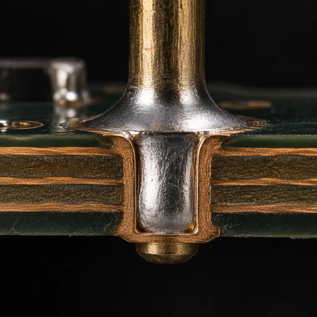
In a conventional mixed-technology flow, the through-hole connectors are placed after reflow — either by hand, by a selective soldering nozzle, or by wave soldering with a pallet masking the SMD side. Each of those adds a separate operation, its own fixturing, and its own yield risk. Pin-in-paste removes the second operation entirely: paste is printed through apertures that overprint the through-hole pads, the connector pins are inserted into a barrel that already contains paste, and the single reflow cycle forms both the SMD joints and the through-hole joints simultaneously.
The economics favour PIP when three conditions hold. First, the through-hole count is modest relative to the SMD count — typically a handful of connectors rather than a dense connector field. Second, the board volume is high enough that the tooling cost of a custom stencil and the engineering time to qualify the process is amortised over many panels. Third, and most important, the connector itself can survive the reflow profile. When those conditions hold, PIP removes a whole process step, its labour, and its associated defect modes. When they do not, selective soldering is the safer choice and remains the industry default for dense through-hole content.
Key Takeaway: Pin-in-paste is a volume and feasibility decision, not a preference. Run the paste volume calculation and check the connector temperature rating first — if either fails, selective soldering is the correct answer, and qualifying PIP anyway will cost more than it saves.
The Paste Volume Equation That Decides Feasibility
This is the calculation most guides skip, and it is where PIP projects are won or lost. The stencil must deposit enough paste to fill the annular volume of the through-hole barrel and form a proper fillet, accounting for the fact that solder paste is roughly half flux and volatile carriers by volume. The printed paste volume therefore needs to be approximately twice the final solder volume required.
Start with the barrel. The volume of the annular space between the pin and the hole wall is:
Vbarrel = π × (rhole² − rpin²) × tboard
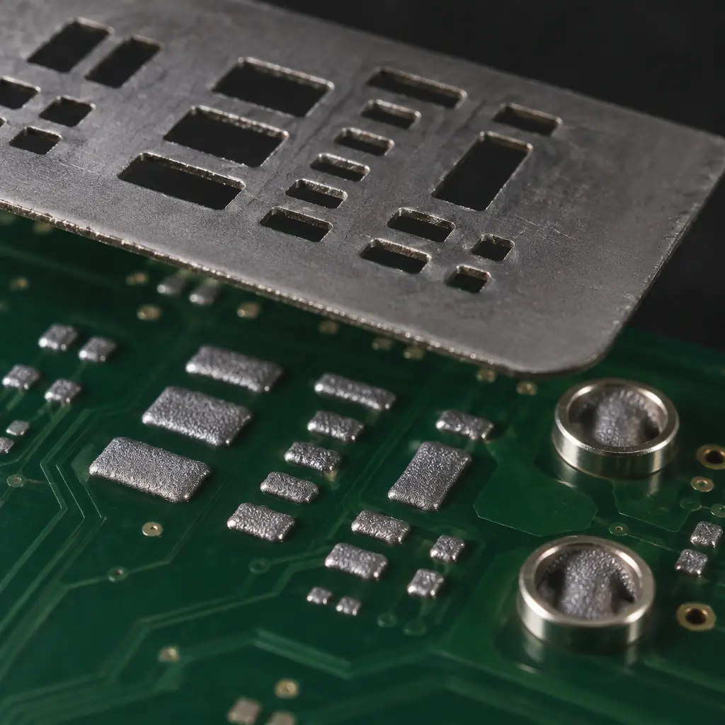
For a nominal 1.0 mm finished hole with a 0.5 mm square pin in a 1.6 mm board, the annulus volume is roughly 0.94 mm³. Add the fillet volume required at the top and bottom of the joint, and add the solder needed to form the toe of each leg. Because the paste-to-solder volumetric shrinkage is close to 50 percent, the paste volume must be about 1.9 mm³ to yield 0.94 mm³ of solder. That paste has to come from the stencil aperture, and the aperture volume is simply area multiplied by foil thickness. With a 0.12 mm stencil, you need roughly 15.8 mm² of aperture area per pin — which is far more than the through-hole pad itself provides. The extra area comes from overprinting onto the pad and the adjacent surface, which is exactly what makes PIP stencil design delicate.
The practical consequence is that PIP needs generous real estate around each through-hole pad to host the overprint area. On a dense connector field, that space often does not exist without crowding neighbouring SMD pads, and the calculation is what tells you so before you cut a stencil. This is the same volume thinking that governs stencil aperture design and paste release for fine-pitch SMD work, applied to a much deeper target.
Stencil and Aperture Design for PIP
With the required paste volume in hand, the stencil design becomes an exercise in delivering it without creating defects elsewhere. The general approach is a stepped or overprinting aperture that extends beyond the through-hole pad onto a defined surrounding area, combined with careful component keep-out management. Four variables carry most of the design:
| Variable | Typical Setting | Effect |
|---|---|---|
| Stencil thickness | 0.12–0.20 mm (often stepped up locally) | Deeper foil delivers more paste volume per unit area |
| Overprint area | Aperture extends 0.3–0.5 mm beyond pad in 2–4 directions | Grows the available volume without a thicker stencil |
| Corner radius | Rounded aperture corners | Improves paste release and reduces bridging |
| Keep-out to SMD pads | ≥0.3 mm from adjacent aperture | Prevents paste bridging between PIP and SMD sites |
Two safeguards matter in practice. First, never let two PIP apertures merge — neighbouring connector pins each need their own controlled deposit, and a merged aperture dumps paste across the connector footprint. Second, verify the paste release behaviour for the specific aperture area ratio; deep PIP apertures have a lower aspect than they first appear and release can be poor without a polished, well-tensioned stencil. The broader principles sit in our guide to SMT stencil design.
Connector Body Temperature Limits: The Real Constraint
Even a perfect paste volume calculation fails if the connector cannot survive reflow. This is the single most common reason PIP is abandoned mid-project, and it is worth checking before anything else. Most plastic-bodied through-hole connectors — headers, terminal blocks, D-subminiature, IDC headers — are rated for a short exposure to reflow temperatures, but the rating is often conditional and easy to overstate.
| Connector Type | Typical Reflow Rating | PIP Suitability |
|---|---|---|
| High-temp nylon headers (LCP/PA9T) | 260 °C peak, 10 s | Good — designed for reflow |
| Standard PA66 terminal blocks | Often 230–250 °C peak or unspecified | Marginal — verify datasheet, expect warpage |
| THT connectors with soft plastic bodies | Frequently no reflow rating | Poor — use selective soldering |
| Metal-shell connectors (D-sub, circular) | Varies with internal insulator | Case by case — insulator governs |
The practical check is to read the connector datasheet for a reflow-temperature exposure rating, not a storage or operating temperature. A connector rated to 105 °C operating and silent on reflow is not PIP-compatible until the supplier confirms it. Where a connector is marginal, the mitigations are a reduced peak temperature with a longer soak, a thermal shield or heat-sink clip over the connector body, or simply accepting the second soldering step for that one part. Assuming all plastic bodies are interchangeable is how PIP projects produce warped, misaligned connectors that pass electrical test and fail mechanical inspection.
Defects to Control in Pin-in-Paste
PIP concentrates several defect modes into one process, and knowing them is how a build is kept in control. The recurring four:
Insufficient fill and open joints
When the printed paste volume falls short of the barrel requirement, the joint forms with a partial or missing fillet. The cause is usually an under-designed aperture or poor paste release, not a reflow fault. Verify the volume equation against the actual deposit with an X-ray or cross-section before scaling.
Bridging between adjacent pins
Overprinted apertures that are too close together, or paste slump before reflow, bridge neighbouring pins. The fix is aperture spacing and keep-out discipline plus a paste with good anti-slump behaviour. Paste choice interacts directly with this, as covered in our solder paste selection guide.
Voiding in the through-hole joint
Volatile carriers in the extra paste volume generate voids during reflow, particularly in thick boards and large barrels. A controlled soak in the profile lets the volatiles escape before the paste fully coalesces. Voiding is inspected by X-ray, the same method used to check BGA and through-hole joints.
Connector warpage and pin misalignment
A connector body heated above its rating deforms, moving the pins and producing joints that look acceptable but do not meet position or coplanarity requirements. This is a thermal-limit problem, not a soldering problem, and the only reliable prevention is placing the connector in the correct rating class at the design stage.
PIP Versus Selective Soldering Versus Wave: Making the Call
The decision between the three through-hole soldering methods reduces to a few observable characteristics of the board. Use pin-in-paste when the through-hole count is low, the connectors are rated for reflow, there is enough board area to host the overprint apertures, and the volume justifies the stencil and process qualification. Use selective soldering when the through-hole content is dense, mixed, or includes connectors that cannot tolerate reflow — it is slower per joint but far more forgiving and needs no paste volume gymnastics. Use wave soldering with a pallet when the board is predominantly through-hole or when a large connector field must be soldered economically at very high volume.
In short: pin-in-paste removes a process step and saves cost when the arithmetic and the connector rating allow it; selective soldering is the robust default when they do not. The two frequently coexist on the same program, with PIP applied to the reflow-rated headers and selective soldering reserved for the temperature-sensitive parts. The cost structure behind that choice is set out in our PCB assembly cost breakdown, and the process step PIP removes is the same one discussed in the comparison of wave versus selective soldering.
Key Takeaway: Run two checks before quoting a mixed-technology board for PIP — the paste volume equation for each connector, and the reflow temperature rating on the connector datasheet. Both must pass. Where they do not, selective soldering on that connector is the lower-risk answer.
Cost and NRE Implications
Pin-in-paste shifts cost rather than simply removing it. It adds engineering time to design and qualify the stencil, an initial process study with cross-section or X-ray verification, and a slightly higher paste consumption per board. It removes a second soldering operation, its labour, its fixturing, and its own defect modes, and it shortens the overall assembly route. On a medium-to-high volume board with reflow-rated connectors, the removal typically outweighs the addition within the first production run. On a low-volume or prototyping board, the tooling and qualification overhead is not amortised, and the savings never appear.
The NRE side is worth planning explicitly: a PIP stencil is not a standard SMD stencil, and the qualification run produces data that should be retained as part of the process record. Buyers evaluating the trade-off against the alternatives should also weigh the tooling economics generally, which follow the same pattern as press-fit assembly, the other common way to avoid soldering a through-hole connector.
At Huaxing PCBA we evaluate pin-in-paste feasibility per board, run the volume calculation against your actual connector footprint, and confirm the connector reflow rating before committing a mixed-technology build to a single-pass process. Boards that fail the check go to selective soldering rather than being forced through reflow. Send your Gerber and BOM with the connector part numbers and we will return a process recommendation alongside the quote, or talk to our engineering team about the right soldering route for your assembly.
