A power distribution network fails in two ways that look identical on a schematic and completely different on a board. The first is not enough capacitance. The second, and the more common, is enough capacitance mounted badly. Two boards with the same bill of materials, the same stackup and the same capacitor count can differ by 20 dB in high-frequency impedance purely because of how far the vias are from the pads and how long the return path is.
This article deals with the second failure. Our power integrity and PDN design guide covers target impedance from first principles; this piece assumes that work is done and asks what happens between the calculated network and the physical board.
Mounting Inductance Is the Real Cap
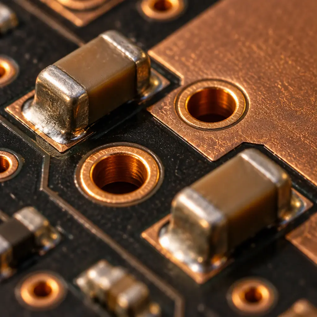
Every decoupling capacitor carries two inductances in series with it: the component's own equivalent series inductance, and the inductance of the path from the pad, through the via, into the plane and back. For a small ceramic part in a 0402 or 0603 package, the second term dominates. Published ESL figures for 0402 ceramics sit around 0.3 to 0.5 nH; the mounting loop from a pair of vias spaced one millimetre apart and drilled through 1.6 mm of board typically contributes another 0.8 to 1.6 nH depending on drill size and plane depth.
| Mounting arrangement (0402, 1.6 mm board, 0.3 mm drill) | Approx. loop inductance | Self-resonance with 100 nF |
|---|---|---|
| Vias directly at pad edges, 0.8 mm apart | 0.9 nH | ~17 MHz |
| Vias 0.5 mm from pad, 1.6 mm apart | 1.4 nH | ~13 MHz |
| Vias at end of 1 mm trace stub, 3 mm apart | 2.6 nH | ~10 MHz |
| Single via shared between two capacitors | 2.0-3.0 nH | ~10 MHz |
The consequence is direct: a capacitor whose self-resonance has dropped to 10 MHz is an inductor above 10 MHz. It is not decoupling anything in the range where most of the fast current transients live. Four capacitors mounted badly do not equal one capacitor mounted well; they equal four inductors.
Rule of thumb: put the via pair first, the pad second, and the trace length at zero. If a layout tool will not allow a via-in-pad, the next best arrangement is a pair of vias placed at the pad edges on opposite sides. A capacitor connected by any trace longer than about 0.5 mm is a capacitor with a series inductor you did not design.
Self-Resonance and the Anti-Resonance Trap
A real capacitor is a series RLC. Below its self-resonant frequency it behaves capacitively; above it, inductively. The resonant frequency scales as one over the square root of inductance times capacitance, which is why a 10 uF part in the same package resonates lower than a 100 nF part. This is the origin of the classic decoupling ladder: a large bulk part for low frequencies, mid-range parts for the middle, and small parts for the high end.
The ladder has a failure mode that simulation models of individual capacitors cannot show. Two capacitors in parallel, with different self-resonant frequencies, form a parallel resonant circuit between their resonances. At the anti-resonance frequency the two branches cancel and the impedance peaks, sometimes by 10 dB or more above either capacitor's own impedance at that frequency. The peak lands precisely in the band the network was supposed to cover.
There are three practical responses. Choose values that are a decade apart or more, so the anti-resonance peak is broad and shallow rather than sharp. Use enough different values that the peaks overlap and cancel each other. Or damp deliberately, with a resistor in series with the mid-range capacitance, which costs DC efficiency but flattens the peak. What does not work is adding more of the same value and hoping, because identical capacitors in parallel shift the whole curve down without removing the peak.
Package Size, Not Capacitance, Sets the Ceiling
The highest frequency a capacitor can usefully decouple is set almost entirely by its package and mounting, not by its value. A 0201 part with a tight via pair can be effective to several hundred megahertz. The same value in an 0603 package with a longer loop is effectively an inductor well before that.
| Package | Typical ESL | Practical upper limit (well mounted) | Note |
|---|---|---|---|
| 0201 | 0.2-0.3 nH | 400-600 MHz | Best high-frequency choice, placement critical |
| 0402 | 0.3-0.5 nH | 250-400 MHz | Good balance of handling and performance |
| 0603 | 0.5-0.8 nH | 150-250 MHz | Use when value or voltage demands the size |
| 0805 and larger | 0.8-1.5 nH | below 150 MHz | Bulk only; do not use for high-frequency decoupling |
This table is the argument for putting small, low-inductance parts close to the load and letting larger parts handle bulk at a distance. It is also the argument against the practice of consolidating BOM lines by replacing several 0402 parts with one larger part: the BOM gets shorter and the high-frequency impedance gets worse, and neither change is visible in a DC test.
Plane Pair Capacitance: When the Stackup Does the Work
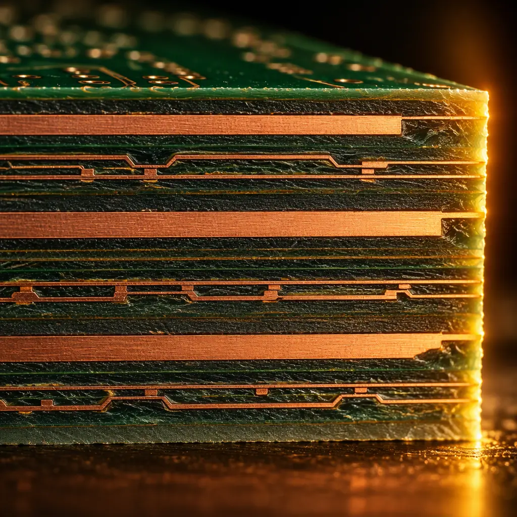
A thin dielectric between a power plane and its adjacent ground plane is a distributed capacitor. Its capacitance per unit area is set by the dielectric constant and the separation, and a 100 micrometre core between two copper planes gives roughly 0.4 nF per square centimetre in FR-4. That sounds small until the area is considered: a 100 by 100 mm board with a full plane pair gives around 40 nF distributed across the entire surface with essentially no mounting inductance, because there is no via in the path at all.
This is why stackup choices made for signal integrity reasons often improve power integrity as a side effect, and why a board with a dedicated thin core between power and ground can need fewer high-frequency capacitors than a board with the same net routed on a thick core. It also explains why plane splits are so damaging: a plane pair interrupted by a split loses the distributed capacitance across the whole interrupted region, not just along the split line.
Measuring It: Two-Port Shunt-Through and VNA Setup
PDN impedance is measurable, but not with the equipment most factories have on the bench. The standard method is a two-port shunt-through measurement using a vector network analyser and two coaxial probes, one injecting current and one sensing voltage, with the ground of both probes connected to the same plane. The measured impedance is derived from the ratio of the two port voltages, and the technique is accurate from a few hundred kilohertz to the gigahertz region if the probes are calibrated at the measurement plane.
- Calibration must be done at the probe tips, not at the cable ends, or the probe inductance appears as part of the network being measured
- A short-circuit calibration with the probes connected to each other sets the floor of the measurement and must be repeated whenever probe spacing changes
- The board must be powered if the measurement is to include DC bias effects on the ceramic capacitance, which means a bias tee or an equivalent injection network
- Probe placement matters more than the analyser specification: measuring at a via far from the load measures the plane, not the load
The result is a curve of impedance against frequency that can be read directly against the target impedance line. Peaks above target are the anti-resonances discussed earlier, and the frequency at which the curve first rises above target tells you where the network stops working.
What a Fabricator Can and Cannot Verify
A board shop can verify that the stackup matches the drawing, that the via geometry is as specified, that plane pairs are continuous and split only where allowed, and that the drilled and plated dimensions are within tolerance. It can also measure plane-pair capacitance on a test coupon and report it. It cannot verify the assembled PDN impedance without a VNA, probes and a powered board, and any supplier claiming to have verified decoupling on a production build should be asked which of those they used.
This distinction matters commercially. A buyer who asks for PDN verification and receives a stackup certificate has been given something real, but it is not what was asked for. The honest answer from a supplier is that impedance verification needs a measurement the customer usually owns, and the useful contribution from the factory is a design that makes that measurement pass.
Specifying PDN Requirements in a Purchase Order
Three requirements are worth writing down. First, the stackup with plane assignments and dielectric thicknesses, controlled as a document rather than as a note. Second, a via policy for decoupling: via count per capacitor, maximum trace length from pad to via, and whether via-in-pad is permitted with what fill and cap. Third, a change-control rule that any substitution affecting the decoupling network requires written approval.
With those in the order, most PDN arguments become checkable facts. The supporting material on stackup design is in our PCB stackup guide, the impedance measurement method in the TDR test coupon guide, and the via geometry constraints in the via aspect ratio article. For products where EMC is the commercial driver, the EMC and EMI compliance guide covers how decoupling choices show up in a test report.
Send Us the Power Nets You Are Worried About
If a board has failed transient testing or a regulator is oscillating under load, send the stackup and the decoupling layout with the schematic net names. We will review mounting inductance and plane continuity before the next build rather than after it, and tell you which of the two failure modes you are looking at.