

A tolerance stack-up is what happens when several individually acceptable dimensions combine into an assembly that does not fit. Each dimension is within its own tolerance, and yet the connector will not seat, the pin misses its pad, or the finished stack is too tall for the housing. PCB design is full of these chains — hole to pad, pad to pad, layer to layer, board edge to feature — and they are easy to overlook because each link looks fine on its own. The discipline of tolerance stack-up analysis is the practice of adding those links up before the board is made, so the assembly is designed to work rather than hoped to work.
What makes PCB stack-up analysis different from mechanical stack-up is that most of the tolerance is generated inside the fabricator, not specified by the designer. Drill position, layer registration, lamination, and routing each contribute their own variability, and the size of that variability is a property of the fabrication process rather than of the drawing. This guide covers why stack-up matters, the fabrication sources of tolerance, the two methods for combining them, a worked connector-alignment example, and the limits a fabricator can actually hold. At Huaxing PCBA we work to the capability limits below across 32-layer fabrication under IATF 16949 and ISO 9001, and we will provide tolerance data for critical features on request.
Why Tolerance Stack-Up Matters in PCB Design
Tolerance stack-up matters whenever a board feature must mate reliably with something else — a component, a connector, another board, or a housing. The classic cases are a connector whose pins must align with plated holes, a press-fit component whose pins must engage holes within a tight band, a board-to-board connector pair whose mating faces must meet at a defined position, and a housing whose opening must align with an edge feature. In each case, the feature tolerances on the board combine with the tolerances of the mating part, and the assembly works only if the sum stays within the clearance available.
The subtlety is that the board's contribution is not one number but several. The distance between two holes depends on where each hole was drilled, which depends on drill position tolerance; the position of a hole relative to a pad depends on drill registration and on layer-to-layer registration for a multilayer board; the position of a feature relative to the board edge depends on routing tolerance. When these are combined without acknowledgment, the result is an assembly that is fine in theory and marginal in production. Making the stack explicit lets the designer choose which links to tighten and which to leave loose, and where to add clearance instead of demanding tighter tolerance.
Key Takeaway: A tolerance stack-up is a design decision, not a manufacturing afterthought. Model the chain before releasing the design, decide which links matter, and where possible add clearance rather than specifying an unnecessarily tight tolerance that raises cost without improving the assembly.
The Sources of Tolerance in Fabrication
The board contributes tolerance at four stages, and knowing them lets a designer allocate the budget correctly.
Drilling. Every hole is drilled at a position with some deviation from nominal, and the drill itself has a diameter tolerance. Drilled hole position is typically held to around ±0.075 mm to ±0.10 mm depending on hole size, board thickness and whether the process is mechanical or laser. Hole size tolerance is typically ±0.05 mm to ±0.075 mm. For high-density designs the drill position dominates the hole-location contribution to any stack that runs between holes.
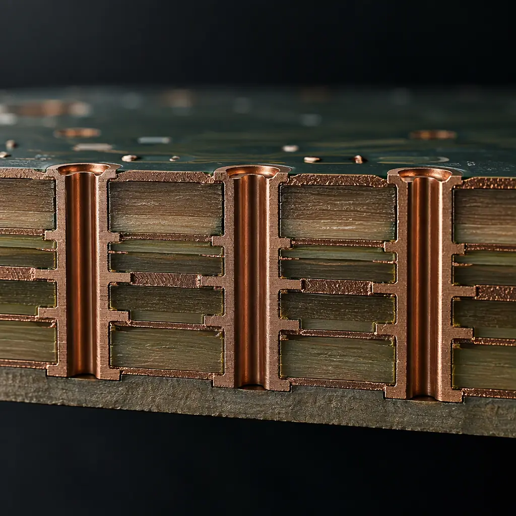
Layer registration. In a multilayer board, each layer is imaged and etched separately and then laminated together. The alignment between layers — layer-to-layer registration — is typically held to around ±0.05 mm to ±0.075 mm on standard processes and tighter on advanced lines. This tolerance determines how far a pad on one layer can sit relative to a pad or plane on another, and it is a major contributor to via annular ring and to any stack that spans layers. Fine-line and high-layer-count designs require tighter registration, which is a capability question rather than a design question.
Lamination and thickness. The thickness of the finished board depends on the laminate and prepreg build, with tolerance on the overall thickness typically around ±10%, and on individual dielectric layers from the material tolerance. This matters for impedance-controlled designs and for any stack where the board thickness feeds the assembly height, such as a board that must fit a slot in a housing.
Routing and edge features. The board outline and any routed features are positioned with their own tolerance, typically around ±0.10 mm to ±0.15 mm for the profile, which matters for edge connectors, board-to-board alignment and housing fit. The completed fabrication drawing collects these, and the practical approach is to ask the fabricator for the achievable tolerance on each feature class rather than assuming a single blanket figure.

Worst-Case vs RSS — Which to Use
There are two standard methods for combining individual tolerances into a stack total, and they answer different questions.
Worst-case (arithmetic sum). The individual tolerances are added directly: if five dimensions each vary by ±0.05 mm, the worst-case stack is ±0.25 mm. This is the conservative method — it guarantees the assembly works even if every dimension simultaneously sits at its extreme. The probability of all dimensions being at their extreme at once is very low, so worst-case analysis can lead to over-tight tolerances and higher cost when applied indiscriminately. It is the right choice when the consequence of failure is severe and the part count in the stack is small.
RSS (root-sum-square). The tolerances are combined as the square root of the sum of their squares: five ±0.05 mm tolerances give √(5 × 0.05²) = ±0.112 mm, roughly half the worst-case figure. RSS is statistically based — it assumes the dimensions are independent and normally distributed, and gives the tolerance within which the stack will fall for the vast majority of units rather than for the theoretical extreme. It is the right choice for high-volume production with many contributors in the stack, where worst-case would demand impossibly tight and expensive individual tolerances. RSS assumes independence and no systematic bias; if the process has a systematic offset, RSS can understate the real variation, so it should be used with a process that is known to be centred.
| Method | How It Combines | When to Use |
|---|---|---|
| Worst-case | Sum of individual tolerances | Small stacks, high consequence of failure, safety-critical |
| RSS | Square root of the sum of squares | Many contributors, high volume, centred process |
In practice, most PCB stacks are analysed both ways: worst-case to establish the guaranteed envelope and identify whether the design works at all, and RSS to understand the realistic production variation and whether tighter tolerances are genuinely needed. Using only worst-case tends to over-specify; using only RSS without checking the worst-case can miss a genuine corner case in a low-volume or safety-critical design.
A Worked Stack: Connector-to-Hole Alignment
Take a connector with pins on a 2.54 mm pitch that must drop into plated holes on the board, where the pin-to-hole clearance allows the pin to be within ±0.15 mm of the hole centre for reliable insertion. The board contributes several tolerances to the position of each hole: drill position ±0.10 mm, and — because the holes must align to a pad on an inner layer for a multilayer board — layer registration ±0.075 mm. The connector itself contributes its own pin-position tolerance, say ±0.10 mm, and the assembly fixture contributes ±0.05 mm.
Worst-case, the position error is 0.10 + 0.075 + 0.10 + 0.05 = ±0.325 mm, well outside the ±0.15 mm clearance — the design fails at worst-case. RSS, the error is √(0.10² + 0.075² + 0.10² + 0.05²) = √(0.01 + 0.0056 + 0.01 + 0.0025) = √0.0281 ≈ ±0.168 mm, still not comfortably inside ±0.15 mm. The analysis shows the design is marginal, and the fix is not to tighten every tolerance — which would be expensive — but to identify the largest contributors. In this case drill position and connector pin position dominate. Enlarging the hole slightly to increase clearance is often the cheapest fix, since it increases the acceptable misalignment without requiring tighter fabrication. If clearance cannot be increased, tightening drill position or specifying a tighter-tolerance connector is the next step.
This example illustrates the value of the exercise: it turns a vague worry about fit into a specific decision about which dimension to change. Without the stack, the natural response to a marginal design is to tighten everything, which raises cost across the board for no targeted benefit. Our related guide on hole accuracy and drilling tolerance covers the drill-side capability in more detail, and the broader manufacturing tolerance guide collects the standard feature limits.
What a Fabricator Can Actually Hold
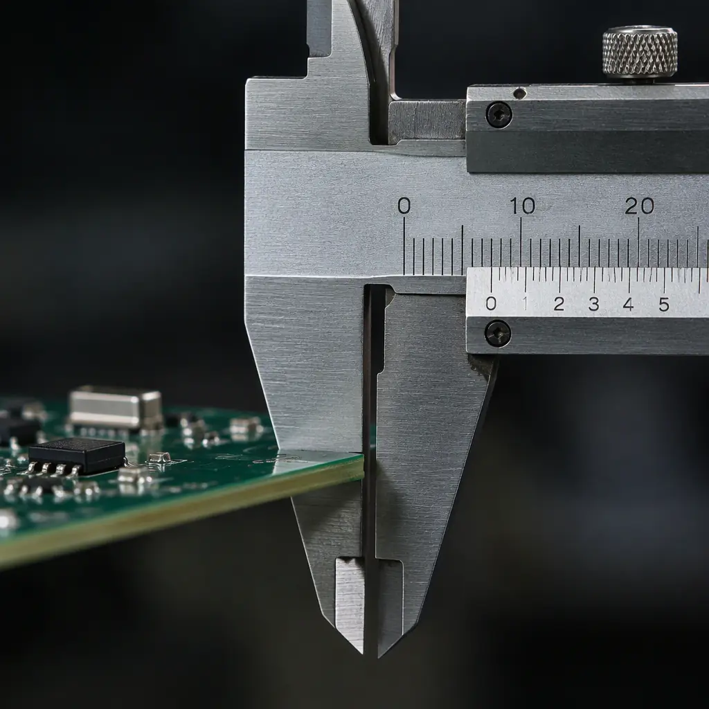
A stack-up is only meaningful if it uses real capability figures rather than textbook assumptions. The following represent typical production capability; the exact numbers depend on board construction and should be confirmed per design.
| Feature | Typical Tolerance | Note |
|---|---|---|
| Drilled hole position | ±0.075 to ±0.10 mm | Hole-to-hole and absolute position; tighter on advanced lines |
| Hole diameter | ±0.05 to ±0.075 mm | PTH finished size tolerance |
| Layer-to-layer registration | ±0.05 to ±0.075 mm | Standard multilayer; tighter for fine-line HDI |
| Board outline (routing) | ±0.10 to ±0.15 mm | Profile position relative to datum |
| Finished board thickness | ±10% typical | Tighter on request for impedance or fit-critical stacks |
The practical rule is to design to the real capability and add clearance where the stack is marginal, rather than to specify tolerances tighter than the process can economically hold. A dimension called out tighter than standard capability raises cost and often cannot be inspected economically, and it is usually more effective to relax a clearance that has margin than to demand a tolerance that has none.
When to Ask for a Tolerance Report
For critical stacks, the cleanest approach is to ask the fabricator for a tolerance report on the specific features that matter before committing to production. A tolerance report states the achievable tolerance on the features in question — hole position, registration, outline — measured on the process that will make the board, rather than quoting a generic catalogue figure. With that data, the stack-up can be run against real numbers, and any mismatch is found before tooling rather than after assembly.
A tolerance report is most valuable for designs with a tight mating requirement, press-fit components, board-to-board connectors, impedance-controlled stacks, and any assembly where a housing fit depends on the finished board profile. It is less necessary for designs with generous clearance, where the standard capability figures are ample. The judgement is whether a stack failure would be caught cheaply before volume or only discovered expensively in assembly, which is the same risk logic that governs the general discipline described in our manufacturing tolerance and stackup design guides.
At Huaxing PCBA we work to the capability limits above across 32-layer fabrication under IATF 16949 and ISO 9001, and we provide tolerance data for critical features and a free DFM review on every quote. Send your Gerber files with the critical dimensions marked and we will confirm achievable tolerances for the features in your stack and return a quote inside 24 hours, or talk to our engineering team about a tolerance-critical assembly.
