
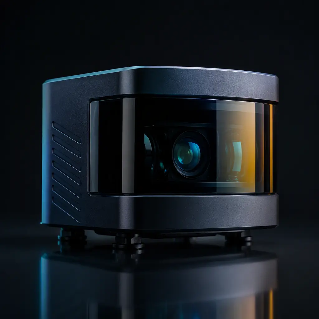
A LiDAR sensor measures distance by firing laser pulses and timing the photons that bounce back. To see a dark object at 200 m, the receiver must detect a handful of photons against sunlight noise, and the whole measurement must complete in nanoseconds. That performance is decided on the PCB: the SPAD detector array's bias and shielding, the laser driver's current loop, the high-speed path that streams millions of points per second, and the thermal control that keeps the sensor honest from a cold highway night to a desert noon.
LiDAR is now a production technology, not a research project, it ships on premium vehicles for ADAS, on AGVs and forklifts in warehouses, on e-scooters for last-mile autonomy, and inside security and survey equipment. Huaxing PCBA assembles LiDAR sensor boards with 0.3 mm pitch BGAs, rigid-flex sections and optical alignment fixtures, and this guide covers the layout decisions our customers iterate on most.
LiDAR Architectures and the Boards They Need
Not all LiDAR is the same, and the architecture determines how many boards the sensor needs and how they are connected:
| Architecture | Scanning Method | Typical Range | Board Impact |
|---|---|---|---|
| Mechanical scanning | Rotating mirror/gimbal | 150–300 m | Rigid-flex + slip-ring or rotary data link |
| MEMS mirror | Oscillating micro-mirror | 100–250 m | Tight driver integration, vibration-sensitive |
| Flash / solid-state | None, flood illumination | 30–100 m | Large SPAD array, huge data bandwidth |
| FMCW | Frequency-modulated beam | 200–400 m | Coherent receiver, high linearity analog front end |
Most automotive and robotics LiDAR in production today is a hybrid: a scanning element (rotating mirror or MEMS) with a SPAD or APD receiver array and a VCSEL or EEL transmitter. The scanning element often lives on a flex or rigid-flex PCB that rotates with the optics, connected to the main compute board through a high-speed rotary link. Our ADAS PCB guide and robotics PCB guide cover the system-level reliability requirements; below are the LiDAR-specific boards.
The Receiver Board: SPAD Arrays and Analog Front Ends
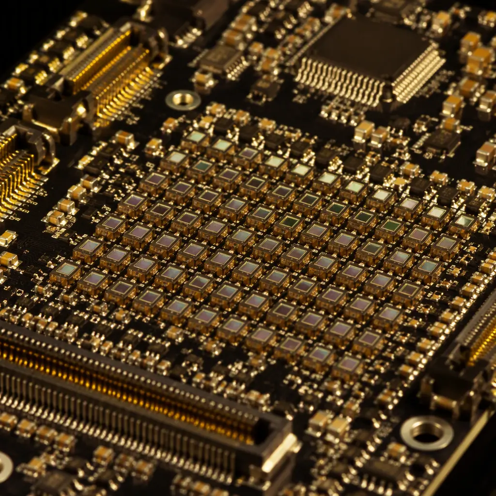
The receiver is the most demanding board in the sensor. A SPAD (single-photon avalanche diode) array must be biased above its breakdown voltage: typically 20–30 V . And its output is a stream of sub-nanosecond pulses that the TDC (time-to-digital converter) timestamps with picosecond resolution.
Clean, noise-free bias generation
The SPAD bias rail is the sensor's dynamic range. Any ripple on the 20–30 V supply appears as timing jitter or false counts. Use a dedicated bias IC with a quiet analog ground island, local bulk and high-frequency decoupling, and route the bias traces as guarded analog lines, never under the digital switching rails. Board-level partitioning guidance is in our mixed-signal PCB guide.
Dark count rate is a temperature and noise problem
SPAD dark count rate (DCR) roughly doubles for every 7–10°C rise in junction temperature. The receiver board must keep the array cool and keep switching noise off the substrate: no digital traces routed under the array, guard rings around the sensitive area, and a thermal path, a copper plane connected to the housing or a TEC, directly under the die. Our thermal management guide covers the plane and via strategy.
Sub-nanosecond routing discipline
SPAD outputs and TDC inputs carry pulses with risetimes under 1 ns. Traces must be short, matched in length, and referenced to a solid ground plane; a 1 mm length mismatch is roughly 5 ps of skew, and at the picosecond timing budgets of modern TDCs that is real error. Keep the analog front end and TDC on the same side of the board, within a few millimeters of each other.
The Transmitter Board: Nanosecond Current Loops
The laser driver switches tens of amps in nanoseconds. A VCSEL array for a flash LiDAR can draw 50–100 A pulses at sub-10 ns risetimes, repeated at kilohertz rates. This is the harshest electrical environment on the sensor, and it lives centimeters from the most sensitive receiver.
Minimize the driver-to-laser loop
Every nanohenry of inductance in the driver loop slows the pulse and wastes optical power. Place the driver die and the VCSEL within millimeters, use wide paired traces or a dedicated layer pair for the pulse path, and put the gate/source return directly beneath the forward path. The switching-loop rules in our SMPS layout guide apply, scaled to nanosecond speed.
Keep the transmitter off the receiver ground
Pulse currents flowing through shared ground create voltage offsets that the SPAD front end sees as noise. Partition the ground planes, transmitter, receiver and digital compute, with a defined single-point bridge or tight stitching along a clean boundary. This is the same discipline used in EMI/EMC design, but at current levels where a few milliohms of shared impedance is fatal.
Eye safety and monitoring circuits
Class 1 eye-safe operation requires the driver to monitor laser current and shutdown within microseconds if the pulse exceeds limits. The monitoring sense resistor and comparator loop must be as tight as the main pulse loop, a monitoring path routed across the board adds latency that defeats the safety function. Functional-safety partitioning for automotive is covered in our ISO 26262 guide.
The Data Path: Streaming Millions of Points Per Second
A modern LiDAR produces 0.5–4 million points per second. Each point carries distance, intensity and timestamp data, so the path from TDC to the host processor is a multi-gigabit link: often MIPI, LVDS or a serialized link such as GMSL2 or PCIe.
Controlled impedance and length matching
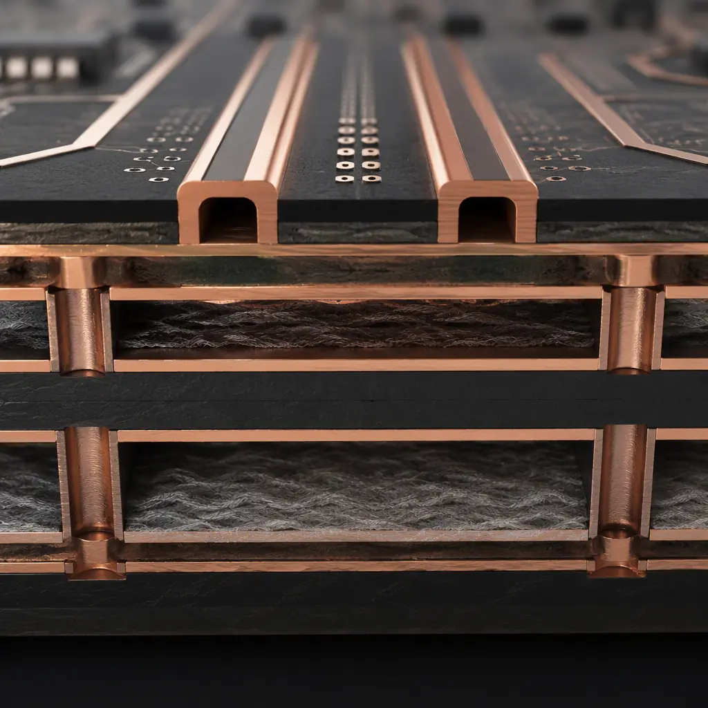
Differential pairs for the data links need 100 Ω controlled impedance with length matching to within a few mils, reference plane continuity under every pair, and no vias in the high-speed lanes unless unavoidable (and then with stitching vias beside them). Stackup and impedance planning is covered in our impedance control guide and high-speed connector guide.
Isolate the compute section from the analog front end
The FPGA or SoC switching at 1+ GHz is a noise source for the SPAD front end. Keep the compute section physically separated, its power fed through a ferrite-bead filtered rail, and the ground plane stitched only at the defined bridge. Data crossing the boundary goes through the level translators or isolation components at one edge of the partition.
Power integrity for burst-mode processing
Point-cloud processing is bursty. The FPGA draws current in frame-rate bursts that can couple into the analog rails. Local bulk capacitance at the FPGA supply pins, a clean power plane, and power-rail separation from the analog sections are the minimum. Our power integrity guide details the decoupling budget.

Thermal and Mechanical Reality in the Field
LiDAR sensors on a vehicle roof or a warehouse AGV face an environment that is simultaneously optical, thermal and mechanical. The board is the thermal backbone.
Laser efficiency means waste heat
VCSEL and EEL lasers convert only 30–50% of input power to light; the rest becomes heat in a small area. A 100 W average optical power transmitter can mean 100–200 W of waste heat that must reach the housing. Plan a thermal path of copper planes and vias from the laser and driver directly to the chassis, and verify with thermal simulation before the mechanical design is locked. Material choices for the path are in our materials guide.
Automotive-grade vibration and temperature cycling
Automotive LiDAR boards must survive -40 to +85°C operation, 20+ g vibration and years of thermal cycling. That means AEC-Q100 components, robust solder joints (premium surface finish, controlled reflow), conformal coating where condensation is possible, and mechanical mounting that does not stress the BGA arrays. Test coverage for these conditions is described in our vibration and shock testing guide and thermal cycling guide.
Optical alignment and the flex sections
Scanning LiDAR uses rigid-flex boards to carry signals across the rotating interface. Flex sections need controlled bend radii, strain relief at the rigid-flex boundary, and plating of the flex fingers, common failure points that our rigid-flex guide covers in detail. Optical components (laser dies, photodetectors, lenses) are aligned after assembly; the board layout must leave the alignment fiducials and access clearances that the fixture needs.
Key Takeaway: A LiDAR sensor is three boards in one fight: a picosecond-precision receiver, a nanosecond-pulsed transmitter, and a gigabit compute section. On a single thermal platform that must hold them all at stable temperature in the field. Every layout decision is a compromise between those three.
Manufacturing and Testing LiDAR Boards
LiDAR boards combine fine-pitch BGAs, mixed analog/RF, rigid-flex and optical alignment, a combination that requires specific process controls.
X-ray and AOI on the fine-pitch and BGA sections
The SPAD array and FPGA are typically 0.3–0.4 mm pitch BGAs. X-ray inspection verifies the solder joints under the array that AOI cannot reach, and SPI validates paste volume before reflow. Our BGA assembly guide and AOI/X-ray/SPI guide cover acceptance criteria.
Functional test with an optical target
Production test needs a calibrated optical target at a known distance and a dark chamber for DCR measurement. Every unit should verify range accuracy, point-cloud density and dark count rate, not just power-on. Test strategy options are compared in our testing methods guide.
First-article alignment and DFM review
Optical alignment tolerances are measured in microns; a DFM review before production catches the layout details, fiducial placement, flex bend radius, component keep-outs, that otherwise appear as yield loss at the alignment station. Our first article guide describes the pre-production verification flow.
Summary: The LiDAR Board Checklist
Treat the sensor as three coupled subsystems: a cool, clean SPAD receiver with picosecond routing; a tight, isolated laser-driver loop with a real thermal path; and a high-speed compute section on controlled-impedance links, all on a rigid-flex platform that survives automotive vibration and temperature cycling. Validate with optical target testing and X-ray on every fine-pitch joint.
At Huaxing PCBA, we assemble LiDAR sensor boards with 0201 passives, 0.3 mm pitch BGAs and rigid-flex sections across 8 SMT lines, with X-ray inspection and optical-fixture alignment support. Our engineering team reviews impedance, thermal paths and flex strain relief during the free DFM check. Read our mmWave PCB guide for the complementary radar side of perception hardware, or contact us with your sensor design for a manufacturing review.
