

The global smart meter market is projected to exceed 1.2 billion installed units by 2028, with Asia-Pacific alone deploying over 600 million AMI (Advanced Metering Infrastructure) endpoints. Behind every smart meter is a PCB that must read sub-milliampere current sensors, survive -40°C winter nights and +85°C enclosure heat, and operate maintenance-free for two decades. If your PCB fails at year eight, the utility replaces the entire meter — and the manufacturer loses the contract.
At Huaxing PCBA, we manufacture smart grid PCBs for meter OEMs and distribution automation suppliers across 12 countries. Our facility handles the full stack: 4-layer to 12-layer mixed-signal designs, high-voltage isolation up to 6kV, conformal coating for outdoor enclosures, and extended temperature qualification from -40°C to +125°C. If you're sourcing PCBs for a smart grid product, here's what to specify in your fabrication notes — and what separates a 5-year board from a 20-year board.
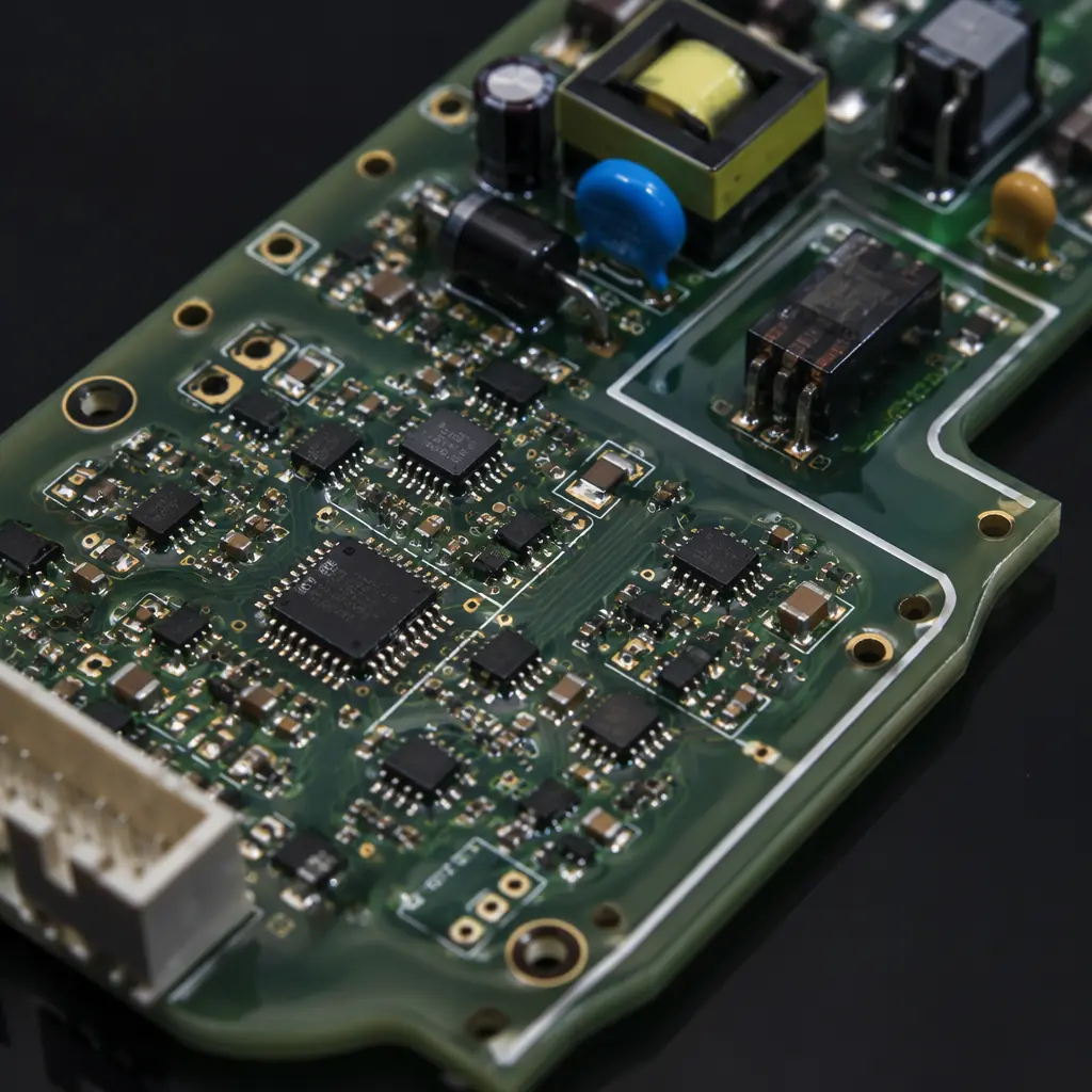
What Makes Smart Grid PCBs Different from Standard Industrial Boards
At first glance, a smart meter PCB looks like any other mixed-signal IoT board — a microcontroller, a cellular or RF module, some current sensors, and a power supply. The difference is in the operating envelope and the reliability math. A consumer IoT device that fails after three years is annoying; a smart meter that fails after three years triggers a truck roll that costs the utility $150-300 and may violate regulatory uptime requirements.
Outdoor Enclosure Thermal Cycling: -40°C to +85°C, 15-Year Minimum
Smart meters in Arizona sun or Canadian winter see daily temperature swings of 30-50°C. Over 15 years, that's over 5,000 thermal cycles. The PCB laminate must have a glass transition temperature (Tg) above 170°C — standard FR-4 with Tg 130°C will delaminate within 3-5 years. See our laminate selection guide for the detailed material comparison. Additionally, CTE (coefficient of thermal expansion) must be matched between the laminate and the heavy copper planes used in the power supply section — a 30 ppm/°C mismatch across a 100mm board creates 45μm of shear stress per cycle.
Mixed-Signal Isolation: Microvolt Analog Next to 240V AC Sensing
A residential smart meter PCB simultaneously measures 240V AC line voltage (through a resistive divider or voltage transformer) and microvolt-level signals from a shunt current sensor. The analog front-end must achieve 80 dB or better CMRR (common-mode rejection ratio), which demands careful PCB layout: separate analog and digital ground planes with a single-point star connection, guard rings around the high-impedance ADC inputs, and at least 6mm creepage distance between the line-voltage section and the low-voltage digital section per IEC 62052-31. Our mixed-signal PCB design guide covers the grounding and partitioning techniques in detail.
Conformal Coating for Humidity, Salt Fog, and Insect Ingress
Outdoor meter enclosures are rated IP54 or IP65, but condensation still forms inside during rapid temperature changes. Without conformal coating, moisture bridges the creepage gaps between high-voltage and low-voltage sections — leading to dendritic growth and eventual short circuits. We apply 50-75μm of acrylic or silicone conformal coating (IPC-CC-830 qualified) to all smart grid PCBs. For coastal installations with salt fog exposure, we recommend silicone-based coating with 2x layer thickness. Read our conformal coating guide for material selection criteria.
20-Year Battery Backup and Ultra-Low Leakage Design
Most smart meters include a lithium-thionyl chloride battery for real-time clock retention during power outages. The PCB's leakage current in the battery circuit must stay below 1 μA at 85°C — even a 10 μA leakage will drain a 2.4 Ah battery in under 30 years instead of the rated life. This requires: no-clean flux residues with SIR (surface insulation resistance) above 100 MΩ after 1,000 hours at 85°C/85% RH, solder mask with high insulation resistance (>5×10¹² Ω), and routing the battery trace on an inner layer away from any switching nodes. Our ionic contamination guide explains the SIR testing we perform on every smart grid production lot.
IEC 62056-21 / DLMS/COSEM Communication Reliability
AMI meters communicate via PLC (Power Line Communication), RF mesh (802.15.4g), or cellular (LTE Cat-M1/NB-IoT). The PCB's controlled impedance traces for the RF section must maintain ±5% tolerance at the operating frequency (868 MHz, 915 MHz, or 2.4 GHz). For PLC designs, the coupling transformer and line filter section requires 4kV isolation between the mains-coupled side and the digital logic side. See our impedance control guide for specifying tolerances in your fabrication notes.
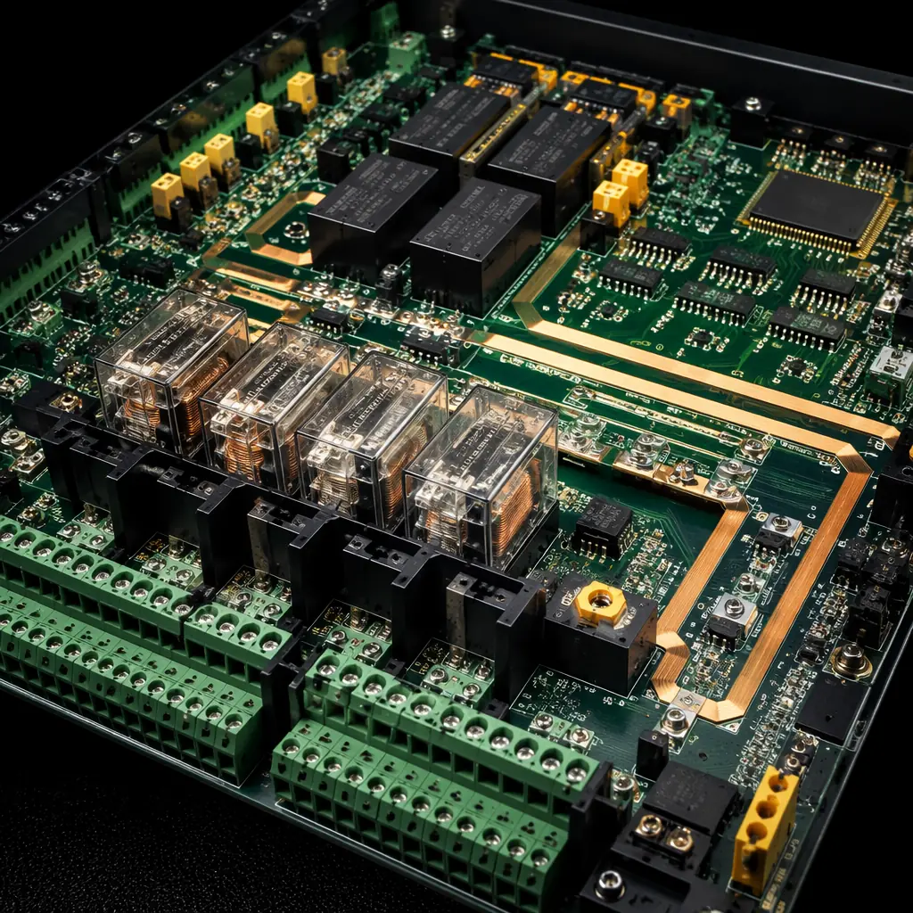
Distribution Automation and Substation Control: The Next Tier of Requirements
Beyond residential smart meters, distribution automation (DA) equipment — reclosers, capacitor bank controllers, feeder RTUs, and substation gateway devices — operates at higher voltages and in even harsher environments. These PCBs sit inside pad-mount enclosures or substation control cabinets where ambient temperatures can reach +70°C and electromagnetic interference from nearby switchgear is severe.
| Parameter | Smart Meter PCB | DA Controller PCB | Substation RTU PCB |
|---|---|---|---|
| Layer count | 4-6 layers | 6-10 layers | 8-16 layers |
| High-voltage isolation | 4 kV | 6 kV | 10 kV |
| Operating temperature | -40 to +85°C | -40 to +105°C | -40 to +85°C |
| Copper weight (power) | 2 oz | 4-6 oz | 3-4 oz |
| EMC standard | IEC 61000-4-2/4/5 | IEC 61850-3 | IEC 61850-3, IEEE 1613 |
| Design life | 15-20 years | 20-25 years | 20-30 years |
For DA controllers and substation gateways, the PCB must also withstand the high transient voltages induced by nearby circuit breaker operations. IEC 61850-3 requires ±4kV fast transient burst immunity and ±2kV surge immunity on all I/O ports — these are tested at the system level, but the PCB layout is the foundation: keep the transient suppression components (TVS diodes, gas discharge tubes) within 25mm of the connector pins, route protection traces on outer layers with wide copper pours to a low-impedance chassis ground, and avoid vias in the discharge path. Our EMC/EMI design guide covers the layout rules that pass these tests on the first iteration.
Key Takeaway: The PCB is the single most common failure point in smart grid field returns — ahead of connectors, displays, and semiconductor components. The three biggest contributors are: (1) laminate delamination from thermal cycling, (2) electrochemical migration from inadequate conformal coating, and (3) solder joint fatigue on large BGA packages. Every one of these is preventable with the right material specification and process control.
How to Specify Smart Grid PCBs: 8 Requirements for Your Fabrication Drawing
When you issue an RFQ for smart grid PCBs, include these eight specifications in your fabrication notes. Skipping any one of them turns a 20-year board into a 5-year board.
Laminate: High-Tg FR-4 (≥170°C) Minimum; Polyimide for DA/Substation
Specify Tg 170°C as the absolute floor. For DA equipment operating above 85°C ambient, step up to polyimide (Tg 250°C) or high-performance hydrocarbon ceramic (Rogers 4350B for the RF layer). Include T260 (time to delamination at 260°C) > 30 minutes and T288 > 10 minutes on the material cert. Our materials guide compares 12 substrates by Tg, Dk, and cost.
Surface Finish: ENIG (ENEPIG for Wire-Bonded Sensor Packs)
Smart meters have a combination of fine-pitch QFN/BGA pads (needing flatness) and connector/push-button contacts (needing durability). ENIG provides both: 3-5 μm Ni, 0.05-0.12 μm Au. If your design includes wire-bonded sensor packages (common in precision metrology ICs), upgrade to ENEPIG — the palladium layer prevents nickel diffusion into the gold wire bond. Our surface finish guide covers all options with shelf-life data.
Solder Mask: LPI, Matte Green or Dark Blue, Double-Coated on High-Voltage Areas
The solder mask on a smart grid PCB is a functional insulator, not just cosmetic. On sections carrying > 50V, we apply a second solder mask coat to achieve ≥40μm thickness, which provides dielectric withstand > 1kV. The mask must pass IPC-SM-840 Class T for long-term outdoor UV exposure. See our solder mask guide for dielectric strength data by type and thickness.
Controlled Impedance: ±5% on All RF and High-Speed Digital Traces
Cellular (LTE Cat-M1 at 700-900 MHz), Wi-SUN (915 MHz), and Zigbee (2.4 GHz) all require 50Ω single-ended or 100Ω differential controlled impedance. Specify the impedance target per net class in your fab drawing and require a TDR (Time Domain Reflectometry) test coupon report with every lot. Full impedance control specification guide here.
Conformal Coating: IPC-CC-830, Full Coverage Including Edge Connectors
Acrylic (AR) for general outdoor use; silicone (SR) for coastal/high-humidity; parylene for the highest-reliability DA/substation applications. Mask off connectors, buttons, and programming pads before coating. The coating must pass the IPC-TM-650 2.6.3.3 moisture and insulation resistance test after 1,000 hours at 85°C/85% RH.
Testing: 100% Flying Probe + AOI; Sample IST for Plated Through-Hole Reliability
Every smart grid PCB undergoes flying probe electrical test (100% netlist verification) and automated optical inspection. For lots above 1,000 units, we include IST (Interconnect Stress Testing) on test coupons per IPC-TM-650 2.6.26 — the plated through-holes must survive 150 cycles from ambient to 150°C with < 10% resistance increase. Our PCB testing methods guide compares every test option by cost and defect coverage.
Via Treatment: Plugged and Capped Vias on All BGA Pads
Via-in-pad is common on smart meter PCBs where the MCU is in a 0.5mm-pitch BGA package. All vias under BGA pads must be filled with non-conductive epoxy, planarized, and capped with copper (IPC-4761 Type VII). Unfilled vias trap flux residues that outgas during reflow and cause voiding under the BGA. Our via fill guide explains each fill type with cross-section images.
Traceability: 2D Data Matrix on Every Board with Lot Code and Date Code
Utility customers require full traceability for field failure analysis — a 2D data matrix (laser-marked on the solder mask) containing the PCB lot number, date code, and panel position. This links every field return directly to the production batch data, including laminate lot, solder paste batch, and reflow profile. See our FAI guide for the traceability documentation package we deliver with every first article.
Why the PCB Manufacturer Matters More for Smart Grid Than for Consumer Electronics
In consumer electronics, a PCB manufacturer change is a cost negotiation. In smart grid, it's a requalification nightmare. Utility customers and metrology labs certify the complete meter design — including the specific PCB manufacturer's laminate supplier, surface finish chemistry, and solder mask brand. Changing any one of these triggers a full recertification cycle that can take 6-12 months and cost $50,000-$150,000 in lab fees.
This is why smart grid OEMs prioritize manufacturers with ISO 9001 and IATF 16949 certifications, documented material traceability from laminate supplier to finished board, and a proven track record of 10+ year production continuity. At Huaxing PCBA, we've manufactured PCBs for smart grid products since 2016, with some designs running unchanged for over 8 years across multiple production campaigns. Read our supplier audit guide for the questions to ask during factory qualification.
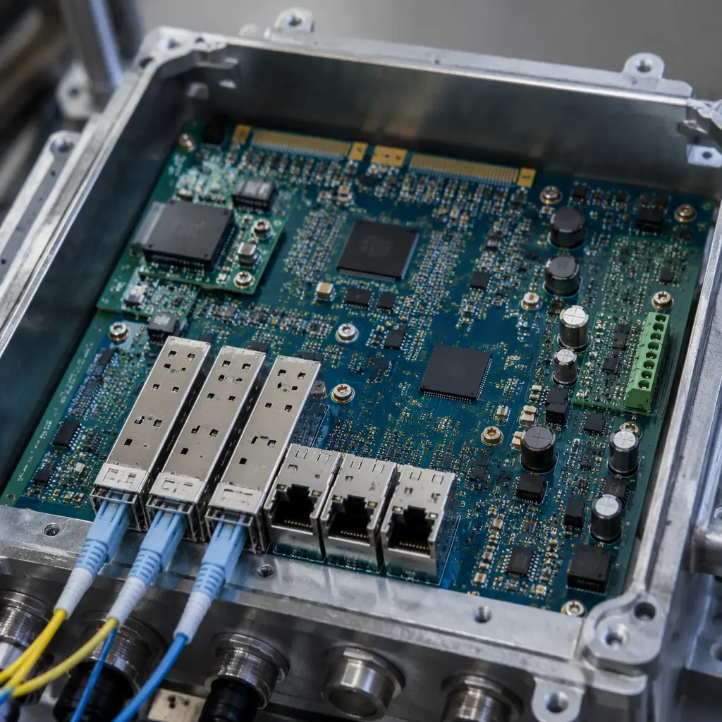
Smart Grid PCB Trends: What's Shaping the Next Generation
Three technology shifts are changing what smart grid PCBs look like. If you're designing a next-generation meter or DA controller, these trends will affect your PCB specification:
Edge AI in the Meter: The latest generation of smart meters (Itron Riva, Landis+Gyr Revelo) includes DSP/accelerator chips for on-meter harmonic analysis, load disaggregation, and arc fault detection — tasks that used to run on a cloud server. These chips (typically ARM Cortex-M7 with DSP extensions or small NPUs) need a clean 6-layer PCB with dedicated power planes and low-ESR decoupling, similar to what we cover in our AI edge computing PCB guide.
Single-Board Design with Integrated Communications: Older meters had separate PCBs for metrology, communications, and display. The new trend is a single 8-10 layer PCB integrating everything — which means careful partitioning of the noisy cellular/PLC section from the sensitive metrology front-end. This is where our experience with mixed-signal PCB design and controlled impedance becomes essential.
Cybersecurity Hardware Root of Trust: Regulatory mandates (NIST IR 7628, IEC 62443) now require a hardware security module (HSM) on the PCB for secure boot and encrypted firmware updates. The HSM IC (often a dedicated secure element like Microchip ATECC608 or NXP EdgeLock) sits on an isolated I²C bus with tamper-detection traces routed on an inner layer — any physical attack shorts the traces and zeroes the keys.
Getting Started with Your Smart Grid PCB Project
Smart grid PCB manufacturing sits at the intersection of precision analog, high-voltage isolation, and long-term environmental reliability — three disciplines that require different expertise, all on the same board. The key is specifying the right materials, testing, and process controls in your fabrication drawing from day one, not discovering field failures five years into deployment.
At Huaxing PCBA, we manufacture PCBs for AMI meters, DA controllers, and substation RTUs with the full certification stack — ISO 9001, IATF 16949, and UL (ZPMV2). Our smart grid production line includes automated conformal coating, 100% flying probe test with 4-wire Kelvin measurement for the current-sense shunt pads, and IST qualification on every laminate lot. See our certifications page for the complete list, or contact our engineering team with your Gerber files and fabrication notes for a project-specific quote with DFM feedback within 24 hours.
