
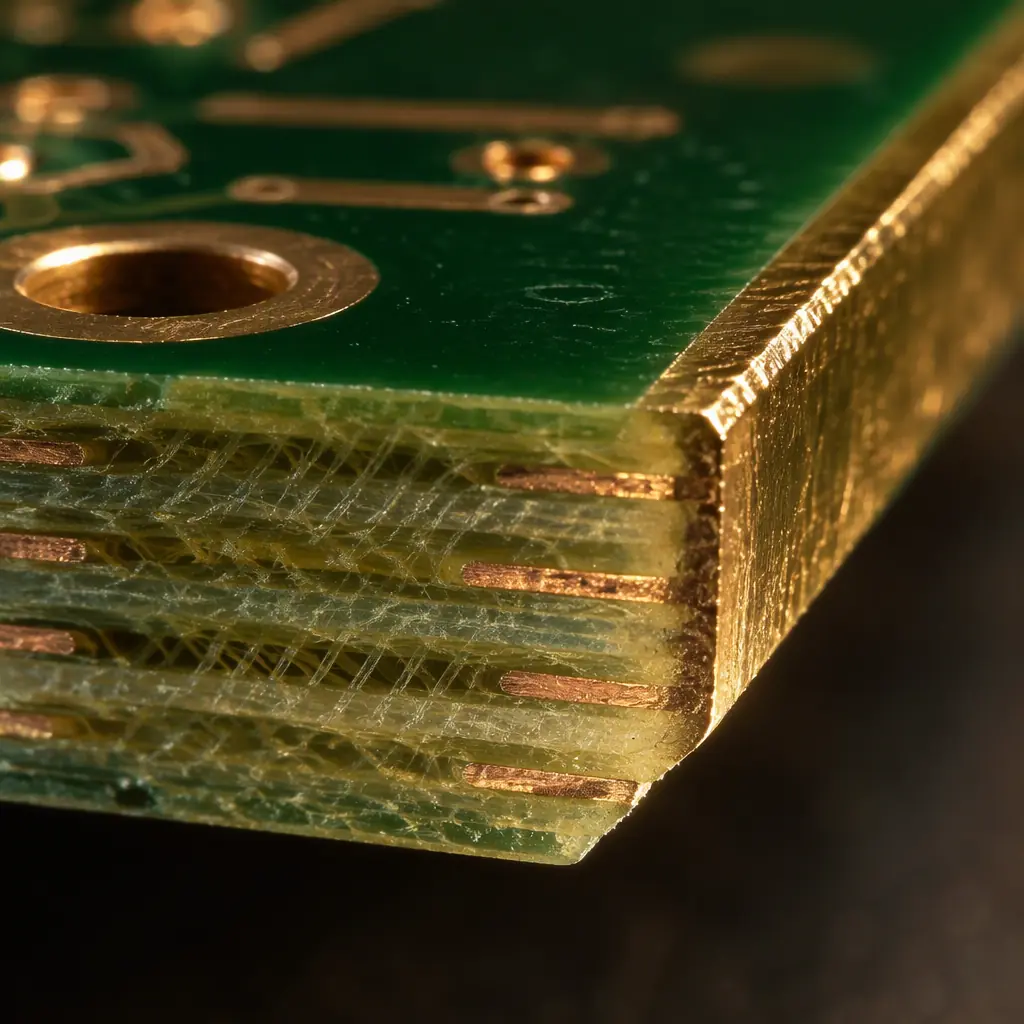
A finished circuit board has four surfaces that matter and three of them are usually specified in detail. The top and bottom carry the copper, mask and finish, and their acceptance criteria are well defined. The drilled features have their own tolerance and plating requirements. The fourth surface is the routed or punched edge, and it is the one that is most often left to the fabricator's default with no requirement written down at all.
That edge is not inert. The routing operation cuts through the laminate and exposes the ends of the glass fibre bundles and the internal plies. Those exposed ends are a path for moisture to wick into the board, and they are mechanically unsupported against the handling and abrasion that assembly, depanelisation and connector mating impose. Whether that matters depends entirely on the environment and the mechanical duty of the product. For a board in a sealed enclosure it usually does not. For a board that is itself the mechanical interface — a card-edge connector, a module that slides into a rail, a product exposed to condensing humidity — it decides service life.
What Copper Wrap Actually Is
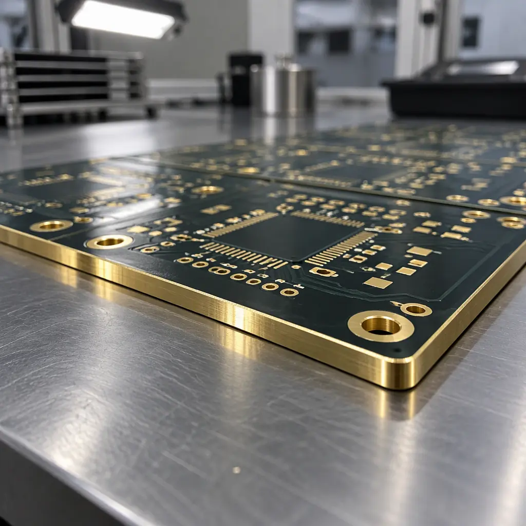
Copper wrap, also called wrap-around plating or edge plating, is the deposition of copper onto the routed edge of a board so that it connects the copper on the top and bottom surfaces around the perimeter. It is not the same as a castellated hole, although the two are often confused because both appear at the board edge and both involve plating a cut surface.
| Feature | What It Is | Purpose |
|---|---|---|
| Copper wrap / edge plating | Continuous plated copper around the routed perimeter, connecting top and bottom copper | EMI shielding continuity, moisture barrier at the cut edge, mechanical edge protection, ground continuity between layers |
| Castellated holes | Plated through-holes cut in half by the routing, leaving a half-cylinder at the edge | Solderable edge pads for module-on-board attachment |
| Bare routed edge | Cut laminate with no plating | Default state when nothing is specified |
| V-scored edge | Shallow scored groove for depanelisation | Panel separation only; not a reliability feature |
| Routed with breakout tab | Edge cut with routed slots and break-away bridges | Panel separation with controlled rough edge at tabs |
The distinction matters commercially because a drawing that says plated edge without saying which feature is meant may get castellated holes, wrap plating, neither, or an argument at incoming inspection. If the intent is electrical continuity around the perimeter, that is wrap plating and it must be specified as such, including the layers it must connect. The design rules for the castellated version are different and are covered in our guide to edge plating and castellations.
When the Edge Requirement Is Real
Wrap plating is justified by one of four functional needs. If none of them applies, the default bare edge is the correct and cheaper answer.
EMI containment around the perimeter
When a board sits inside a metal enclosure and the enclosure halves must make electrical contact to form a continuous shield, the board edge is often the structure that carries that contact. Wrap plating connecting top and bottom ground planes around the perimeter gives the shield a continuous conduction path at the board boundary rather than relying on discrete gaskets or finger stock alone. In this application the plating must be connected to the ground network on both surfaces with adequate via stitching, not simply present on the edge.
Moisture ingress control at the laminate edge
Cut glass-reinforced laminate exposes fibre bundles that can wick moisture along the fibre-resin interface into the board interior. The effect is slow and becomes relevant in long-life products in humid or condensing service — outdoor equipment, marine electronics, instrumentation that runs for a decade. A plated edge does not make the board hermetic, but it blocks the exposed fibre ends and substantially reduces the wicking path. This is the application most often overlooked, because the failure appears years into service and is attributed to general humidity rather than to an unprotected edge.
Mechanical protection for a handling-exposed edge
Where the board edge is inserted, slid, clamped or repeatedly handled, laminate alone chips and delaminates at the cut. A plated or wrap-covered edge spreads the contact load and resists the edge chipping that produces loose laminate fragments inside an assembly. This is the dominant justification in module and card applications where the edge is a handling surface rather than a connector.
Ground continuity between surface planes
Some designs use the board edge as a low-inductance connection between the top and bottom ground planes, particularly in RF and high-speed boards where via inductance at the perimeter matters. Here the requirement is not just that copper exists on the edge but that it is continuous and tied into the ground network at defined intervals. That is an electrical requirement and should be stated as one, with the maximum stitching interval given.
How to Specify It So It Gets Built and Verified
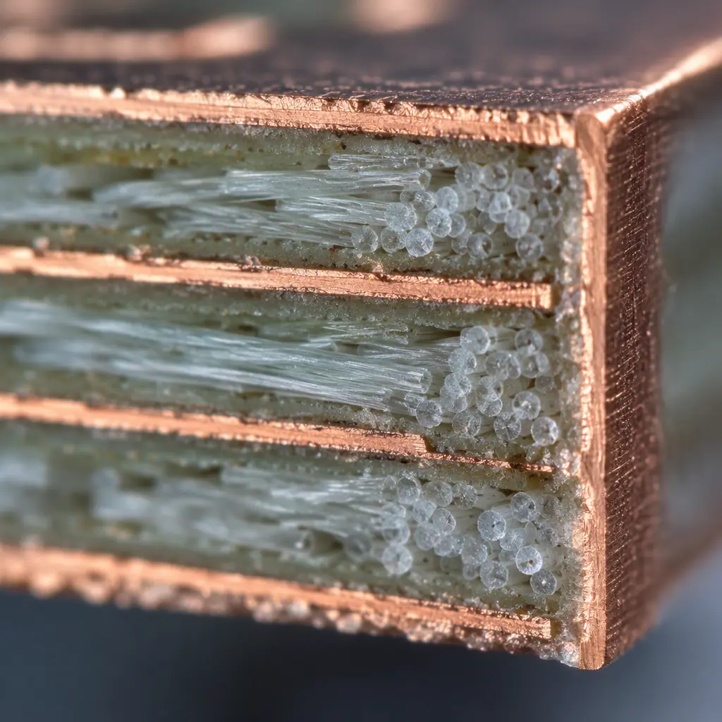
The reason wrap plating is inconsistently delivered is almost always that the requirement was written in a way that cannot be inspected. A drawing note that says plated edge without a defined width, layer connection and measurement point leaves the fabricator to interpret, and interpretation varies.
| Parameter | Why It Must Be Stated | Typical Practical Range |
|---|---|---|
| Which edges are wrapped | Full perimeter vs selected edges changes cost and fixturing significantly | All four edges, or named edges only |
| Plated width onto the surface | Defines the inspection measurement; too narrow risks lifting, too wide intrudes on routing | 0.5 to 2.0 mm of copper on the top and bottom surface adjacent to the edge |
| Copper thickness on the edge | Determines current capacity and mechanical durability | Typically 20 to 35 um finished, matched to surface copper where continuity is the goal |
| Layers to be connected | A wrap that connects only the outer layers is not the same as one that ties internal planes | Name the specific layers, or specify stitching vias inside the wrap band |
| Edge finish | Bare copper on the edge oxidises and is not solderable; finish affects solderability and shelf life | Plated with the same finish as the board surface, or deliberately left as plated metal |
| Stitching via interval | Controls the inductance of the perimeter connection, which matters at RF | Stated as a maximum spacing, typically a fraction of the wavelength of interest |
| Acceptance criteria | Defines what counts as a reject so inspection has a basis | Reference the applicable acceptance standard and state the maximum permitted discontinuity |
Key Takeaway: The single most common specification defect is stating a plated edge without stating the width of copper that must appear on the top and bottom surfaces adjacent to it. Without that number there is nothing to measure, so verification defaults to a visual impression and the requirement becomes unenforceable. State the width, state the layers, state the acceptance criterion.
Fabrication Constraints to Respect
Wrap plating is achievable on standard multilayer construction, but it interacts with several other fabrication steps, and designs that ignore the interaction end up with either a cost premium or a rejected lot.
Panelisation and the edge itself. A board whose edge must be plated cannot be separated from its neighbours by a bare routed slot in the usual way, because the edge being plated must be accessible for plating before separation. This usually means the plated edges face outward toward the panel boundary, with the separation features placed on the other sides. Design teams that assume any edge can be wrapped discover during manufacturing that the panel layout has to change, which is a layout change and a schedule impact. Raising the requirement before panelisation is designed avoids it entirely.
Soldermask registration at the edge. The mask must stop short of the wrap band on the surface, or the wrap is cosmetically present but electrically and mechanically isolated from the surface copper. The mask-to-wrap gap is a real dimension and should be given a tolerance. Where the design also uses mask-defined pads near the edge, the two requirements can conflict, and the wrap band wins only if it is stated as a higher-priority requirement.
Routing tolerance and the wrap edge quality. The routed edge is not a precision feature on a standard board. Router positional tolerance, tool wear and entry and exit marks all affect the edge straightness. A wrap specification that demands a perfectly uniform plated band on a router cut edge is demanding more than the process normally delivers. Where edge quality genuinely matters, it should be stated and paid for, with the tolerance given, rather than assumed as part of a general plating note.
Interaction with high-layer-count builds. On a thick, high-layer-count board the edge area is larger, the exposed internal copper is more numerous, and the risk of an internal plane shorting to the wrap band rises. That is not a reason to avoid wrap plating, but it is a reason to state which internal layers may be exposed at the edge and which must be pulled back. The layer pull-back at the board edge is normally set by the fabricator's capability, and it should be confirmed against your drawing rather than left implicit. Our guide to PCB stackup design covers the copper pull-back conventions, and the general tolerance framework is set out in PCB manufacturing tolerances.
Acceptance and Inspection
An edge requirement that is not inspected is not a requirement. Edge plating has its own failure modes, and each has a visible signature that a defined inspection step can catch.
| Defect | Signature | Consequence If Shipped |
|---|---|---|
| Incomplete wrap coverage | Bare laminate visible within the specified wrap band | Loss of shielding continuity; open moisture path at the gap |
| Wrap not connected to surface copper | Mask or a gap isolating the edge band from the surface plane | Electrically inert edge that looks correct at a glance |
| Lifted or peeling edge plating | Adhesion failure of the band from the laminate | Progressive delamination; loose metal debris inside the assembly |
| Edge plating cracking after depanelisation | Cracks in the band at separation points or near tab locations | Open circuit on the perimeter; intermittent shielding failure |
| Internal layer short to wrap band | Unintended internal plane in contact with the wrap | Short between nets that were meant to be isolated |
| Oxidised or discoloured edge metal | Bare copper edge without the specified finish | Poor solderability if the edge is a solderable surface; cosmetic and corrosion concerns otherwise |
The inspection question worth asking your fabricator is not whether the edge is plated but how they verify the wrap band width and the connection to the surface copper, and whether the verification is recorded per lot. Visual confirmation at a defined magnification with a stated measurement point is adequate for width and coverage. Continuity of the wrap to the surface plane is usually verified electrically, by resistance measurement at defined points around the perimeter. Both are inexpensive to add at first article and both are meaningless if added only verbally. The structure of a first-article approval is described in our guide to first article inspection.
What to Write into the Purchase Specification
Procurement Tip: Put five lines in the specification. First, which edges require wrap plating and which do not. Second, the minimum width of plated copper required on the top and bottom surfaces adjacent to each wrapped edge. Third, the specific layers the wrap must connect, or the maximum stitching via interval if the requirement is electrical. Fourth, the finish required on the plated edge. Fifth, the acceptance criterion for continuity and the inspection method used to confirm it, including whether results are recorded per lot. A supplier who has these five lines will build it correctly and can prove it. Without them you are relying on a drawing note that says plated edge and hoping both sides meant the same thing.
There is also a cost conversation worth having explicitly. Wrap plating adds process steps and constrains panelisation, so it carries a real premium and it is worth paying only when a functional need justifies it. The cheap and correct answer for many boards is a bare routed edge with a clean cut. If your design does not have an EMI continuity requirement, a long-life humid service environment or a mechanically exposed edge, the specification should say clearly that no edge plating is required — which is itself a useful statement, because it prevents a supplier from adding cost and process risk to satisfy an ambiguous drawing note.
The Bottom Line
Copper wrap is a reliability feature for the one surface of a circuit board that most designs leave unspecified. It earns its cost when the board edge carries EMI continuity, sees long-term humidity, is handled mechanically or provides ground continuity between surface planes, and it is wasted cost elsewhere. Where it is needed, it is only obtained reliably if the requirement states the wrap band width, the connected layers, the finish and the acceptance criterion, because those four numbers are what make it measurable. Specified that way, it is a controlled feature. Left as a drawing note, it is a hope.
At Huaxing PCBA we review edge requirements at DFM, flag designs where a wrapped edge interacts badly with the intended panelisation, build the feature with the wrap band width and layer connections recorded on the fabrication drawing, and verify continuity and coverage at first article and per lot according to the agreed criterion. Where a programme does not need edge plating, we will say so rather than add it. Read our edge plating and castellated holes guide or contact our engineering team to review your board edge requirements before fabrication.
