
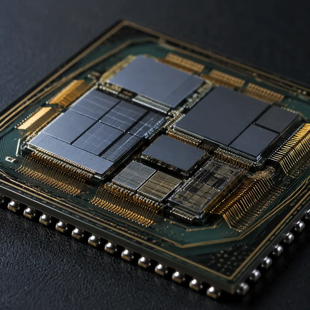
Every few years the PCB industry gets handed a new word that promises to collapse the distance between silicon and board. Chiplet is the current one. The problem is that a great deal of “chiplet” content reads more like a semiconductor press release than a specification a hardware team can build against. The practical reality is far more concrete: chiplet is a way of splitting one large monolithic die into several smaller dies, then co-packaging them so the electronics side of your product can buy silicon that was never designed as a single piece.
What makes this a PCB question and not just a silicon question is the substrate. A chiplet assembly needs a precise, high-density interconnect between dies, and that interconnect lives on a package substrate or interposer that is, structurally, a very sophisticated printed circuit board. It is why this belongs in a conversation about board manufacturing rather than only GPU architecture slides. At Huaxing PCBA we hold 3/3 mil trace, 0.075 mm laser vias and ±5% impedance on up to 32-layer any-layer HDI, the precision tier where substrate technology and advanced board capability actually meet.
Setting the Terms Straight: Chiplet, 2.5D, 3D-IC
The three terms are related but not interchangeable. Getting the taxonomy straight is the single fastest way to have a useful conversation with a supplier.
| Term | What it is | The packaging substrate role | Typical pitch |
|---|---|---|---|
| Chiplet | Split a large die into several smaller dies | Reconnect dies on a package substrate | 40-100 µm microbump | 2.5D | Dies sit side-by-side on an interposer | The interposer is an ultra-high-density board | 10-45 µm in the interposer | 3D-IC | Dies stacked vertically with TSVs | TSV carries signal through the silicon | <20 µm TSV | Fan-out | Dies embedded in a molding compound | RDL rebuilt outward, no separate substrate | 5-20 µm RDL |
The key distinction: chiplet describes how the silicon is partitioned, while 2.5D and 3D-IC describe how the dies are physically arranged and connected. A supplier can quote you “chiplet-ready” and mean any one of these. So always pin down whether you are talking interposer, fan-out, or TSV before you compare any two quotes. For a related read on how advanced packaging intersects with boards, our flip-chip & IC packaging substrates guide covers the front half of this story.
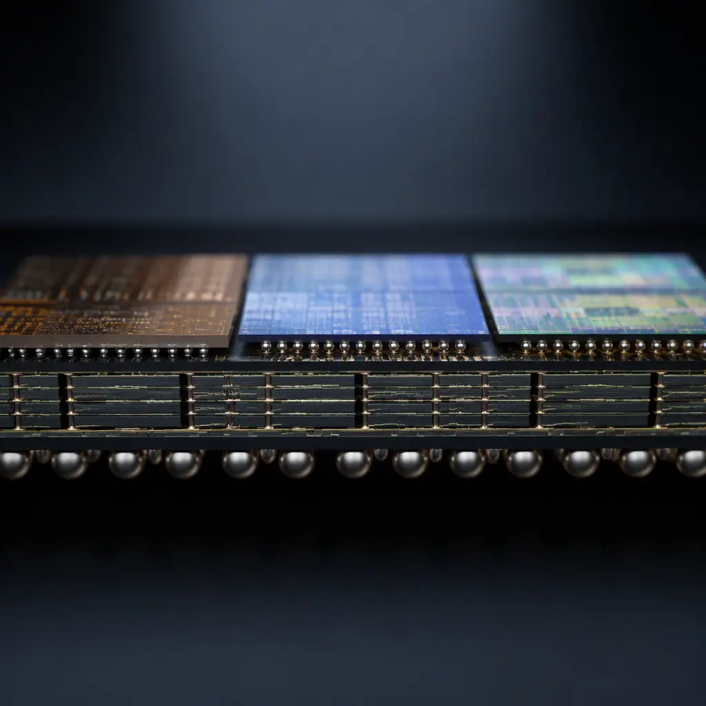
The Substrate Is the Problem, and It Is a Precision Problem
A 2.5D interposer is not a normal PCB. It is a substrate that carries differential pairs at a pitch a tenth of what a conventional board allows, and the tolerance that matters is the truth of where the metal actually sits. The capabilities people quote are meaningless unless they can hold them in a real production environment:
Line and space: where the fight happens
A conventional board is measured in mils. 3/3 mil is already a high-end number, and our limit is 3/3 mil. A package substrate is measured in micrometres. When a substrate vendor quotes 3–5 µm lines, that is roughly ten times finer than an advanced PCB. The gap between those two worlds is where the realistic, buildable boundary sits.
Microvia and RDL density
Fan-out and 2.5D rely on micro-vias and redistribution layers reworked far from the board's own via technology. Our 0.075 mm laser via is the high end of conventional PCB via capability, enough to carry a co-packaged or photonic board, but not a full interposer.
Impedance and controlled dielectric
Whether the substrate is organic or silicon, the differential impedance must hold across a very small cross-section. Our impedance control discipline, built over ±5% on high-speed boards, is the same reasoning applied at a smaller scale.
Important Framing: No single supplier does both a 5 µm interposer and a mainstream board. The honest question for a hardware team is whether your product genuinely needs the interposer tier, or whether an advanced HDI board, the tier Huaxing operates in, gets you 95% of the performance at a fraction of the complexity.
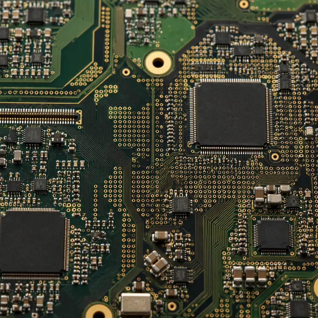
Where the Board Fab Ends and the OSAT Begins
This is the boundary that confuses most buyers. A printed circuit board fabricator (PCB fab) and an outsourced semiconductor assembly and test provider (OSAT) are different businesses.
| Stage | Who owns it | What it delivers |
|---|---|---|
| Die fabrication | Foundry | The silicon dies themselves | Substrate/interposer | Substrate specialist or advanced PCB fab | The high-density carrier | Die-to-substrate attach & encapsulation | OSAT | Microbump, underfill, molding, test | Final board assembly | PCB fab / EMS | Routing to the system board |
At Huaxing PCBA we do not claim the OSAT step. What we do is the board that carries the co-packaged or chiplets-based module onto the system, plus the high-density assembly and test around it. And we are honest about that boundary because a supplier that over-claims capability is a supplier you cannot trust with a tolerance-critical job. For how our co-packaged optics and HDI work extends toward this, those guides are the closest adjacent read.
The Honest Cost-and-Timing Reality
The strongest argument against chasing chiplet packaging is usually economic, not technical. It is worth saying plainly:
A fan-out or interposer substrate is expensive, has long lead times, and requires a supply chain that most mid-volume hardware programs simply do not need. For the vast majority of products, an industrial controller, a medical device, a robotics driver, an IoT edge node, a well-designed high-layer any-layer HDI board delivers the required performance at a fraction of the packaging cost. Chiplets are justified by economics at scale (high-volume compute, AI accelerators, advanced networking) where die yield and silicon reuse pay for the extra packaging. Ask whether your volume and cost model clears that bar before you let the buzzword drive your stackup.
Procurement Tip: Challenge the chiplet requirement with a cost model. If a supplier cannot show you where the packaging cost is recovered in die yield or silicon reuse over your actual bill of materials, the advanced HDI tier is the defensible, buildable answer.
What to Ask a Substrate or Board Supplier
When you evaluate a supplier for a co-packaged or chiplets-based program, the questions below separate a real capability from a marketing slide:
What is the smallest line/space you hold, and in production?
3/3 mil is the number Huaxing builds and guarantees. Any supplier that talks in micrometres for a normal PCB is telling you they are selling packaging, not boards, confirm which one you actually need.
Where is the boundary of your process?
Get an explicit statement of the substrate line they do not cross. A clear “we do this, not that” is more useful than a vague “advanced packaging capable.”
What is the impedance tolerance and via capability?
The measurable, verifiable numbers, ±5% impedance, controlled dielectric, minimum via, are the real signal. Our PCB via technology guide lists the exact figures we ship.
How is the module qualified and tested?
Microsection, X-ray for the BGA, thermal cycling and electrical test are the acceptance evidence. Our cross-section & microsection analysis guide shows what that evidence should look like.
Summary: Buy the Tier You Need, Not the Buzzword
Chiplet and 2.5D packaging are real, and they are advancing how premium silicon ships. But they are a packaging decision made on cost, volume and performance, not a board decision made on hype. The sustainable path for most hardware teams is the high-density, high-precision board tier that a quality PCB fabricator can actually hold in production. That is the tier where the physical limits, buildable trace, via, and impedance, are honest.
At Huaxing PCBA we hold 3/3 mil trace, 0.075 mm laser vias, ±5% impedance and up to 32 layers of any-layer HDI across 8 SMT lines in a 15,000 m² facility serving 30+ countries under ISO 9001, IATF 16949 and UL. Bring us your co-packaged or high-density design for an honest DFM review of where the buildable boundary is. Upload your files or talk to our engineering team about your substrate and stacking specification.
