
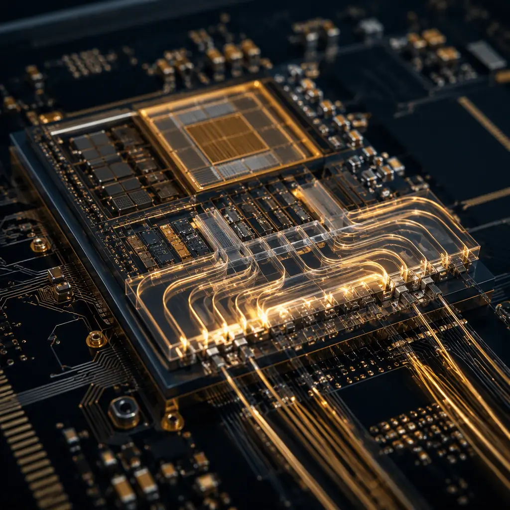
Every switch generation the interconnect distance problem gets harder. At 800G and 1.6T, the electrical link from the switch die to a pluggable optical module over a faceplate is consuming more power and more of the silicon budget than the optics themselves. That is the argument for co-packaged optics (CPO): put the laser and the photodetector on the same substrate as the switch ASIC, and the electrical lane becomes an interposer-die trace instead of a board trace to a connector.
The result is a genuinely different PCB problem. Huaxing PCBA builds 2-32 layer boards down to 3/3 mil line and space with ±5% impedance control, so we are used to the kind of layer count and registration CPO demands.
What Co-Packaging Actually Changes on the Board
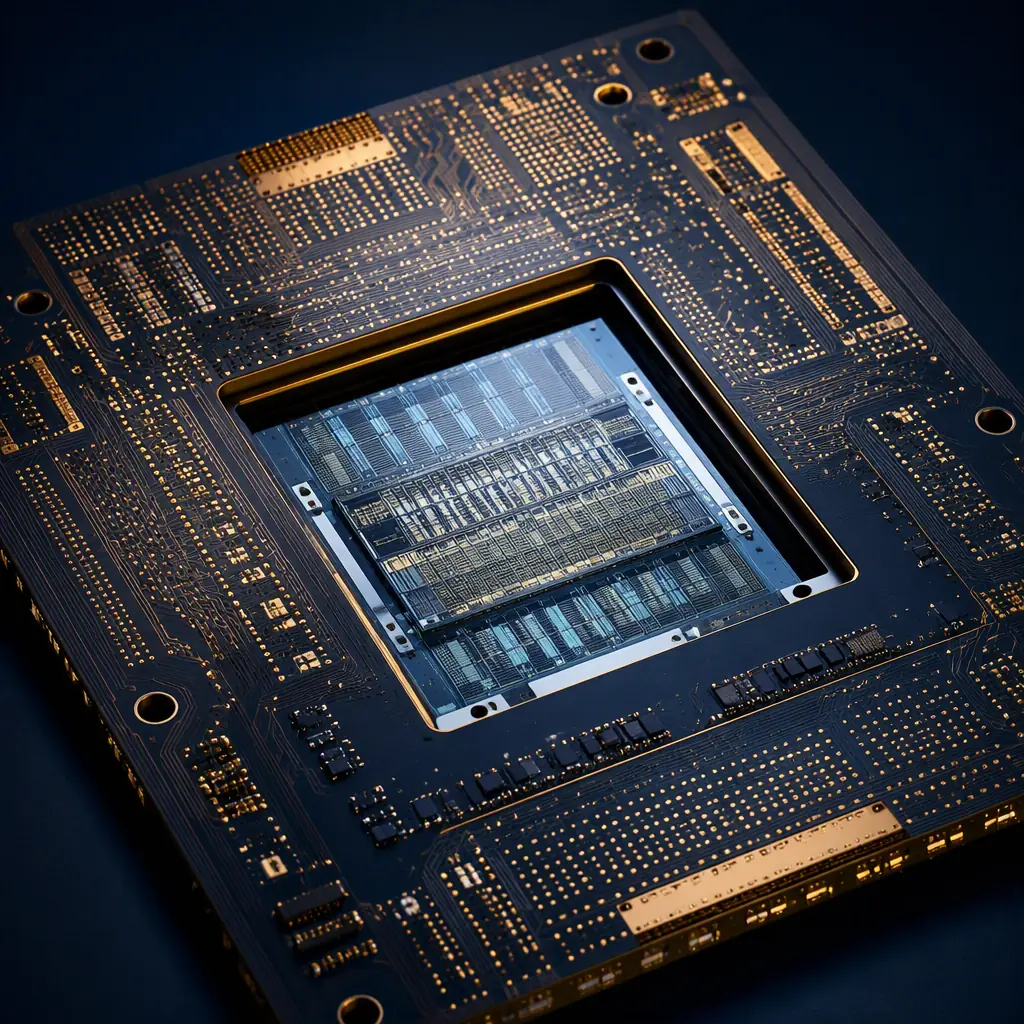
Co-packaged optics does not just re-route a few signals. It redefines where the laser lives, and therefore what the substrate must be. Compare the two architectures:
From Pluggable Modules to an Optical Engine
In a traditional line card the optical module is a QSFP-DD or OSFP pluggable, and the board only routes high-speed differential pairs up to the cage. In a CPO switch, the optical transceiver is a silicon-photonics engine that is edge-coupled or flip-chipped to the switch package, either on the same package or on a very short, very controlled interposer. The board no longer routes 224G traces to a faceplate connector, and that is exactly the point.
Layer Count Goes Up, Not Down
Removing the connector does not reduce routing complexity. The switch die and the optics still fan out to power, ground, and high-speed lanes, but now those lanes are co-located on one substrate. Combined with the fan-out of the switch ASIC in ball-grid-array form, the practical result is a 20-40 layer board with dense any-layer microvia stacks in the core region.
The Laser Needs to Run Cool and Clean
Silicon photonics is efficient, but the laser diode and the driving electronics still dissipate real heat, and the optical bench must stay within a tight temperature window to hold wavelength and link performance. That thermal constraint lands directly on the substrate and its copper thermal paths. See our thermal management guide for the fundamentals.
Choosing Laminate and Stackup for 224G SerDes
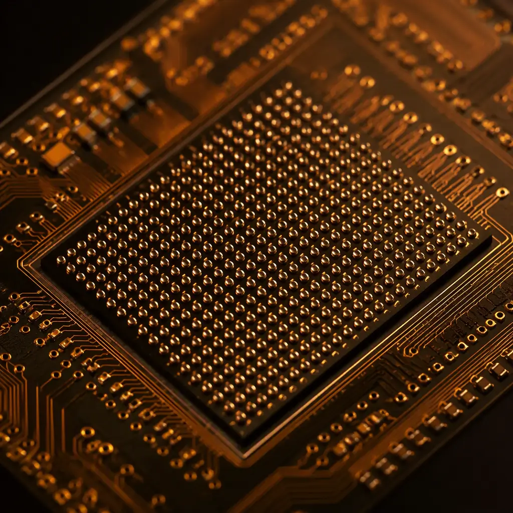
At 112G and 224G per lane, the copper and dielectric losses dominate the channel budget. You cannot get there with a garden-variety FR-4. The insertion loss budget at 224G is roughly 25-40 dB, and most of it is spent before the trace reaches the optics.
Ultra-Low-Loss Laminate, Not Standard FR-4
Standard FR-4 at 224G has a dissipation factor (Df) around 0.020, which destroys the eye. CPO substrates use ultra-low-loss or very-low-loss materials with a Df below 0.003 at 10 GHz. Compare that against the material trade-offs in our PCB materials guide and our laminate selection guide.
Broadside Coupling and Back-Drill Discipline
The stackup must control impedance across broadside-coupled differential pairs while keeping vias stub-free. Back-drilling removes the unused drill stub that would otherwise resonate. See our back drilling guide and our stackup design guide for the mechanicals.
Layer Count and Any-Layer HDI
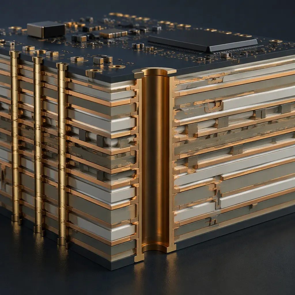
To keep the reference planes continuous and the breakout clean, CPO substrates routinely push 32 layers or more with any-layer microvias. This is exactly the kind of build Huaxing supports with any-layer HDI and fine-pitch BGA fan-out.
| Parameter | CPO Recommendation | Why It Is Set Here |
|---|---|---|
| Signal layer count | 24 – 40+ | Continuous reference planes under dense fan-out |
| Laminate Df @10GHz | < 0.003 | Keeps 224G insertion loss inside budget |
| Impedance tolerance | ±5% | Huaxing standard controlled-impedance spec |
| Minimum line / space | 3/3 mil | Fine-pitch breakout under the ASIC and optics |
| Microvia diameter (any-layer) | 0.075 mm laser | Stub-free vertical interconnects |
Power Integrity and the Co-Packaged Thermal Budget
The switch ASIC and the laser share one substrate, so the power-delivery and thermal problems are coupled. This is where a board can fail not because of signal integrity but because the plane and via design cannot feed a high-current, low-voltage core cleanly.
Low-Impedance Power Delivery
The switch core and the laser drivers need a well-designed power delivery network (PDN) with low impedance across the band of interest. That means thick copper planes, short return paths, and a well-planned decoupling strategy. Our power integrity guide walks through the plane and decoupling rules.
Heavy Copper for the Hot Spots
Where the ASIC and the optics concentrate heat, heavier copper is used to spread it into the thermal vias and the package. See our heavy copper guide for how copper weight changes current-carrying and thermal behavior, and our trace width and current capacity guide for sizing.
Controlled Impedance Across Every Breakout
Signal integrity on a CPO substrate is won or lost in the breakout, not in the far trace. The transition from the ball grid to the trace must keep the differential impedance consistent. Our signal integrity guide covers the breakout and transition rules in detail.
Manufacturing and Inspection of a CPO Substrate
The tolerances in a co-packaged design push manufacturing into territory that ordinary PCB vendors cannot hold. Registration, plating, and inspection all get more demanding.
Registration and Layer Alignment
With 30+ layers and 3 mil traces, layer-to-layer registration is the difference between a working substrate and a pile of open vias. Huaxing controls registration tightly across the build, which matters more as layers stack up.
Microvia Integrity and Reliability
Any-layer microvia stacks must be reliably plated and free of voids. Microvia reliability under thermal cycling is a real risk; trust our microvia reliability guide for the IST and testing approach.
Optical Cleanliness of the Cavity
Because the optical engine sits so close to the substrate, contamination on the surface can degrade the optical path. A clean assembly, appropriate surface finish, and controlled handling are all part of the spec. Our PCB cleaning guide and surface finish guide cover the options.
Summary, Specifying a Co-Packaged Optics Board
Co-packaged optics turns the switch substrate into a photonic assembly. To make it work: pick an ultra-low-loss laminate with a Df under 0.003, build 24-40 layers with any-layer microvias and back-drilled stubs, control impedance to ±5%, and treat power integrity and thermal as a single coupled design. Then hold tight registration and optical-cleanliness standards through manufacturing and inspection.
At Huaxing PCBA we build 2-32 layer boards down to 3/3 mil with ±5% impedance control on 8 SMT lines, and our quality system is certified to IATF 16949, ISO 9001 and UL. We run a free DFM review on high-layer, high-speed and optical substrates, so you can catch a layer-count or material decision before it becomes a yield problem. Send your files for a quote or talk to an engineer about your CPO switch and networking substrate.
