
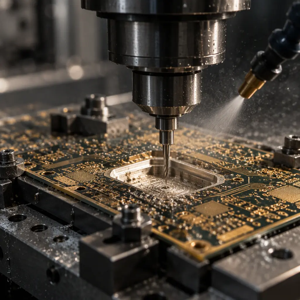
Cavities are one of the least discussed but most useful features in advanced PCB fabrication. A cavity is simply a recessed region in the board — a pocket milled or built into the stack-up so that a component, a shield, a connector or a module can sit below the surface of the board rather than on top of it. They appear in RF modules where a shield lid must sit flush, in products where total stack height is constrained, in sensor packages where an embedded die sits inside the board, and in designs where a recessed connector must align with a housing opening. What makes cavities difficult is not the concept but the manufacturing method, because the choice of how the cavity is made determines the tolerances you can hold, the grounding options available, and the cost.
This guide covers why a cavity is specified, the fundamental choice between a laminated and a machined cavity, the grounding implications of plated versus unplated cavity walls, step-cavity boards for recessed and ZIF connectors, the tolerances a fabricator can actually deliver, and the cost drivers behind it all. At Huaxing PCBA we fabricate cavities and step features alongside conventional routing and machining across 32-layer capability under IATF 16949 and ISO 9001, and the limits below reflect what the process can hold in production rather than in a brochure.
Why Specify a Cavity at All
A cavity solves one or more of four problems, and it is worth being explicit about which one applies because it drives the design. The first is height: a component that must sit below the board surface, either to fit within a housing or to keep the overall product slim, needs a recess to occupy. The second is shielding and RF: a metal shield lid that must sit flush with the board surface, forming a grounded enclosure, is commonly seated in a shallow cavity so the lid and the board form a continuous plane. The third is embedding: a die, a passive component or a sensor placed inside the board stack-up rather than on the surface requires a cavity to accept it. The fourth is connector alignment: a board-edge or mid-board connector that must meet a housing opening at a defined height is often recessed into a step so the mating face lands exactly where the mechanical design expects it.
Each of these use cases narrows the fabrication choice. A flush RF shield wants plated cavity walls for grounding. An embedded component wants a controlled depth and a known dielectric thickness beneath it. A recessed connector wants a repeatable step height so the mating face lines up on every unit. Being clear about the purpose at the start prevents a design that is technically a cavity but functionally unusable.
Key Takeaway: State the purpose of the cavity — height, shielding, embedding or connector alignment — before choosing a fabrication method. The purpose dictates whether the walls must be plated, whether the depth must be tightly controlled, and therefore whether a laminated or machined cavity is appropriate.
Laminated Cavity vs Machined Cavity: The Core Decision
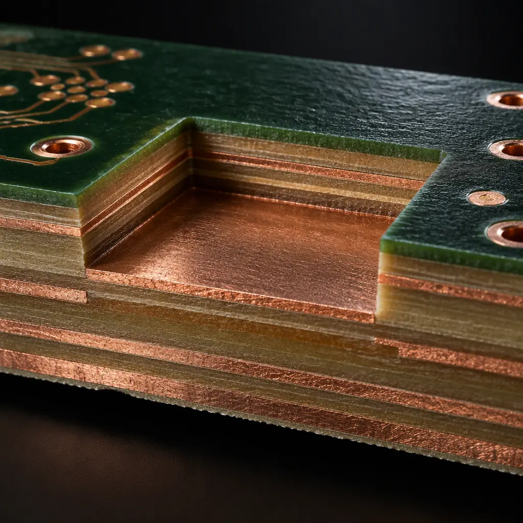
There are two fundamental ways to create a cavity, and the choice is the most consequential decision in the whole design. A laminated cavity is built into the stack-up: the layers are cut with an opening before lamination, so that when the board is pressed the cavity exists as a formed recess bounded by the surrounding dielectric. A machined cavity is routed after lamination: the board is built as a solid multilayer panel and the cavity is milled out of the finished surface, either partially into the depth or through to an inner layer.
| Attribute | Laminated Cavity | Machined Cavity |
|---|---|---|
| When formed | Before lamination, into the layer set | After lamination, into the finished board |
| Depth control | Set by layer thickness — very repeatable | Set by routing depth — needs tolerance management |
| Wall surface | Dielectric, can be plated if designed in | Machined dielectric, plating only if re-processed |
| Best suited to | Deep cavities, embedded components, controlled dielectric beneath | Shallow shields, recessed connectors, tight-zoned routing |
| Cost driver | Layer preparation and lamination complexity | Machining time and yield loss on the routed board |
The rule of thumb is that deep cavities and cavities needing a precisely controlled dielectric beneath them are laminated, while shallow cavities and recesses for connectors and shields are machined. Machined cavities are quicker to introduce and need no special layer preparation, but routing into a laminated, assembled multilayer panel risks delamination at the cavity edge and limits how deep the cut can safely go. Laminated cavities avoid the routing risk and give excellent depth control, but add layer-preparation and lamination steps and are consequently more expensive for a simple shallow recess. Choosing the heavier method for a light application is the most common way cavity designs become unnecessarily costly.
Plated vs Unplated Cavity Walls and Grounding
Whether the cavity wall is plated is a decision with direct electrical consequences, and it is frequently overlooked until the RF or EMC test fails. An unplated cavity wall is bare dielectric — fine for a pocket that holds a component with no electrical function. A plated cavity wall has copper deposited onto the wall, connecting to a net (usually ground), which turns the cavity into a grounded enclosure for shielding, or provides shielding continuity around a component.
For RF modules with a metal shield lid, plated walls are what make the shield work. The lid is soldered or pressed to a plated rim, the rim connects through vias to the internal ground plane, and the cavity plus lid forms a continuous grounded enclosure. Without plating, the lid floats or grounds only through a few points, and the shielding effectiveness is drastically reduced. For embedded components, plated walls can provide a reference plane close to the device, which matters for high-frequency or high-impedance circuits.
The trade-off is process complexity. A laminated cavity that must be plated requires the wall to be metallised as part of the plating process, which means the cavity edges need to be properly prepared and the plating must reach into the recess — a more demanding process than plating a flat surface. A machined cavity cannot easily be plated after the fact without re-entering the plating line, so a machined cavity that needs plated walls usually means the cavity is machined to reveal pre-plated inner-layer features, or the design relies on vias and a separate ground path instead. Deciding the grounding requirement early is what allows the fabricator to choose a method that can actually deliver it, and it sits alongside the broader shielding considerations covered in our guide to hybrid RF stackups.
Step-Cavity Boards for Recessed and ZIF Connectors
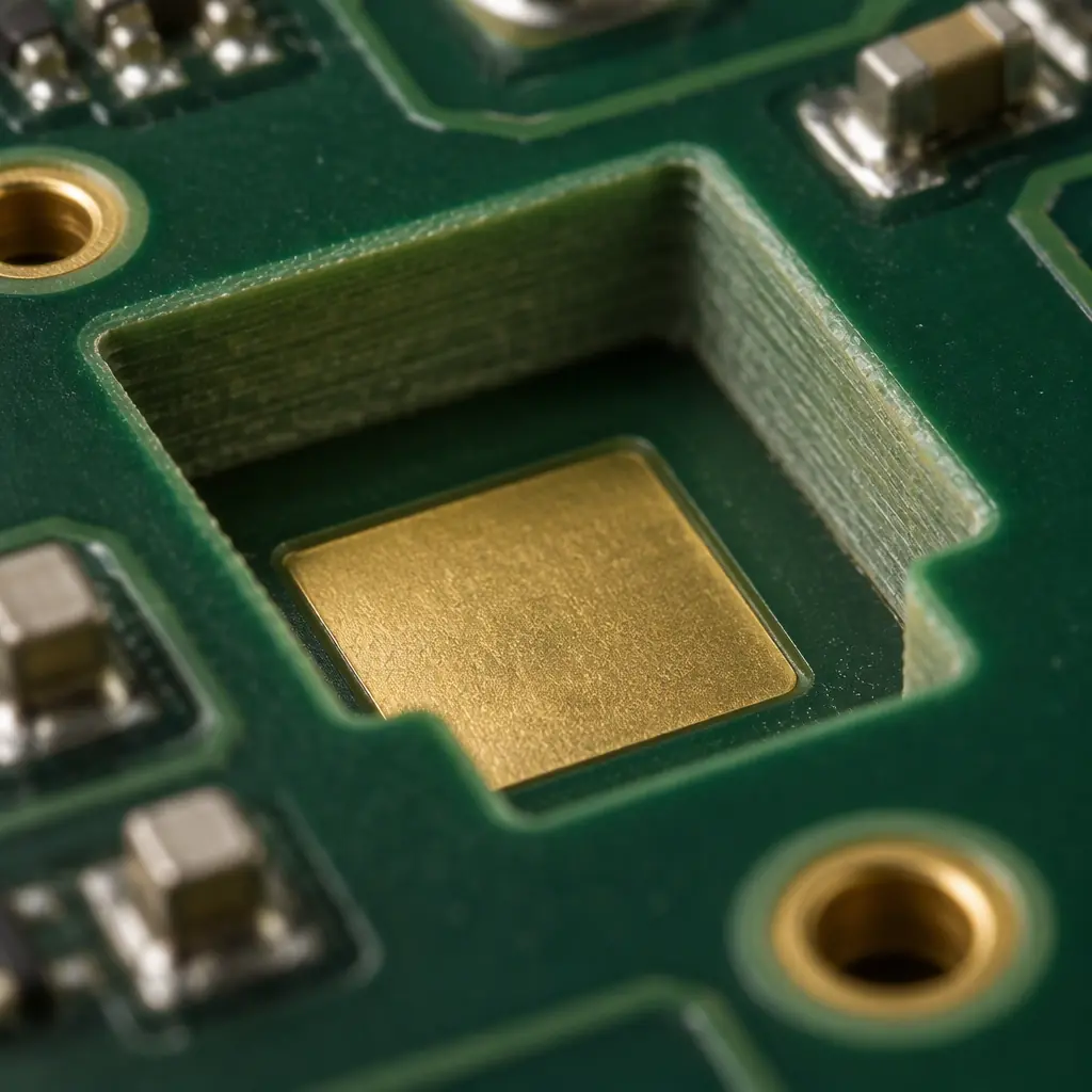
A step cavity is a cavity with more than one depth level — a staircase rather than a single pocket. Step-cavity boards are used when a component or connector must sit at a precise intermediate height, or when a recess must accommodate both a component and the clearance for its mating part. The classic application is a recessed connector, where the board must present a connector face at an exact height to meet a housing opening, and the step provides both the recess and the alignment.
Zero-insertion-force connectors are a frequent driver: a ZIF connector's actuator needs clearance to open and close, and the cable or flex it accepts needs a defined path, so the board is stepped to provide both. Similarly, board-to-board connectors, camera modules and display connectors are often stepped so the mating face lands flush with a housing. The design rules for step cavities are more demanding than for a single-depth cavity because each level must be controlled independently, and the transition between levels must be machined without damaging the surrounding features.
Practical guidance for step cavities: define each step depth relative to the board surface rather than to the previous step, so tolerance does not stack; keep the step transition radius consistent with what the router can cut; and provide a keep-out around each step for the machining operation, since the cutter needs clearance and the surrounding copper must survive. Where the step is used purely for mechanical alignment, an unplated machined step is usually sufficient and much cheaper than a plated laminated step. The related family of machined features — countersinks, counterbores and edge profiles — is covered in our guide to machined PCB features.
Tolerances and Capability Limits
Cavity tolerances are where a design meets reality, and they are tighter than most designers assume. The figures below represent typical production capability for machined and laminated cavities; the exact numbers depend on board thickness, cavity size and layer count, and should be confirmed per design.
| Feature | Typical Tolerance | Note |
|---|---|---|
| Machined cavity depth | ±0.10 mm | Depth measured from board surface; tighter available at cost |
| Laminated cavity depth | Set by layer thickness, ±0.05 mm typical | Very repeatable; the dielectric beneath is well controlled |
| Cavity wall position | ±0.075 to ±0.10 mm | Wall location relative to datum |
| Minimum cavity dimension | Dependent on router bit and depth | Smaller cavities need smaller tooling and shallower cuts |
| Dielectric beneath cavity | Must be defined and confirmed | Critical for embedded components and impedance control |
Two risks deserve emphasis. The first is warpage: a cavity removes material asymmetrically, which changes the mechanical balance of the board and can cause bow and twist during reflow. Designs with large or deep cavities should be reviewed for panel layout and stiffening, and the same warpage discipline that applies to warpage prevention applies here. The second is delamination at the machined cavity edge, where routing into a laminated multilayer can expose the layer interface. A laminated cavity avoids this entirely; a machined cavity should keep the cut clean and away from the layer edges, and the fabrication review should flag any cavity that cuts close to an internal feature.
Cost Drivers
The cost of a cavity is driven by three things: the method, the depth, and the area. A machined cavity costs machining time proportional to the volume removed and the number of depth levels, plus the yield impact of routing into a laminated panel. A laminated cavity costs the layer preparation and the lamination complexity, which is largely fixed per design rather than per unit, so it becomes economical at volume and expensive for a one-off. A step cavity costs more than a single-depth cavity because each level is a separate operation.
The practical cost guidance for a buyer or designer is to specify the shallowest cavity that does the job, to use a machined cavity for simple shallow recesses rather than paying for lamination, and to reserve laminated and plated cavities for the cases that genuinely need controlled depth or grounding. Cavities that are deeper than necessary, or plated when the wall is not electrically used, are the two most common sources of avoidable cost. The general machining and tolerance framework that these costs sit within is discussed in our guide to machined PCB features.
Design Checklist Before You Send Gerbers
The following checks prevent the majority of cavity-related rework. Each corresponds to a decision the fabricator will otherwise have to make for you, usually in the least convenient way.
State the cavity's function
Height clearance, RF shielding, component embedding or connector alignment. The function dictates method, plating and tolerance.
Choose laminated or machined explicitly
Do not leave it to the fabricator. Deep or controlled-dielectric cavities want lamination; shallow recesses want machining.
Decide plated or unplated walls
Plated for grounding and shielding; unplated for mechanical pockets. A plated cavity must be designed as such from the stack-up.
Define depth relative to the board surface
Not relative to the previous step, and not to an inner layer, unless that layer is itself datum-controlled. This prevents tolerance stacking.
Provide machining keep-outs
The router needs clearance around the cavity. Copper, traces and components too close to the wall risk damage or shorting after plating and machining.
Review warpage and panel balance
A large or asymmetric cavity changes the board's stiffness. Confirm the panel can survive reflow without excessive bow and twist.
Confirm the dielectric beneath the cavity
For embedded components and impedance-critical areas, the remaining dielectric thickness must be defined and verified, not assumed.
Key Takeaway: Specify the shallowest cavity that meets the functional need, choose machined for shallow mechanical recesses and laminated for deep or grounded ones, and define every depth and keep-out explicitly. Cavity cost comes from method, depth and area — control all three and the design stays economical.
At Huaxing PCBA we fabricate machined and laminated cavities and step features up to 32-layer HDI capability under IATF 16949 and ISO 9001, with DFM review that flags cavities whose depth, plating or keep-out will not survive production. We will tell you which method suits your application before quoting, so the design is not committed to an expensive route unnecessarily. Send your Gerber files with the cavity purpose and depth requirements and we will return a fabrication recommendation and quote inside 24 hours, or talk to our engineering team about a cavity or embedded-component design.
